LH168M 데이터 시트보기 (PDF) - Sharp Electronics
부품명
상세내역
제조사
LH168M Datasheet PDF : 17 Pages
| |||
LH168M
FUNCTIONAL OPERATIONS OF EACH BLOCK
BLOCK
FUNCTION
Shift Register
Used as a bi-directional shift register which performs the shifting operation by CK and
selects bits for data sampling.
Data Latch
Used to temporary latch the input data which is sent to the sampling memory.
Comparator
Convert low voltage input signal into internal [CMOS level] voltage input signal.
Sampling Memory
Used to sample the data to be entered by time sharing.
Hold Memory
Used for latch processing of data in the sampling memory by LS input.
Level Shifter
Used to shift the data in the hold memory to the power supply level of the analog circuit
unit and sends the shifted data to DA converter.
Reference Voltage
Generation Circuit
Used to generate a gamma-connected 64 x 2-level voltage by the resistor dividing circuit.
DA Converter
Used to generate an analog signal according to the display data and sends the signal to
the output circuit.
Output Circuit
Used as a voltage follower, configured with an operational amplifier and an output buffer,
which outputs analog signals of 64 x 2 gray scales to LCD drive output pin.
INPUT/OUTPUT CIRCUITS
VCC
I
GND
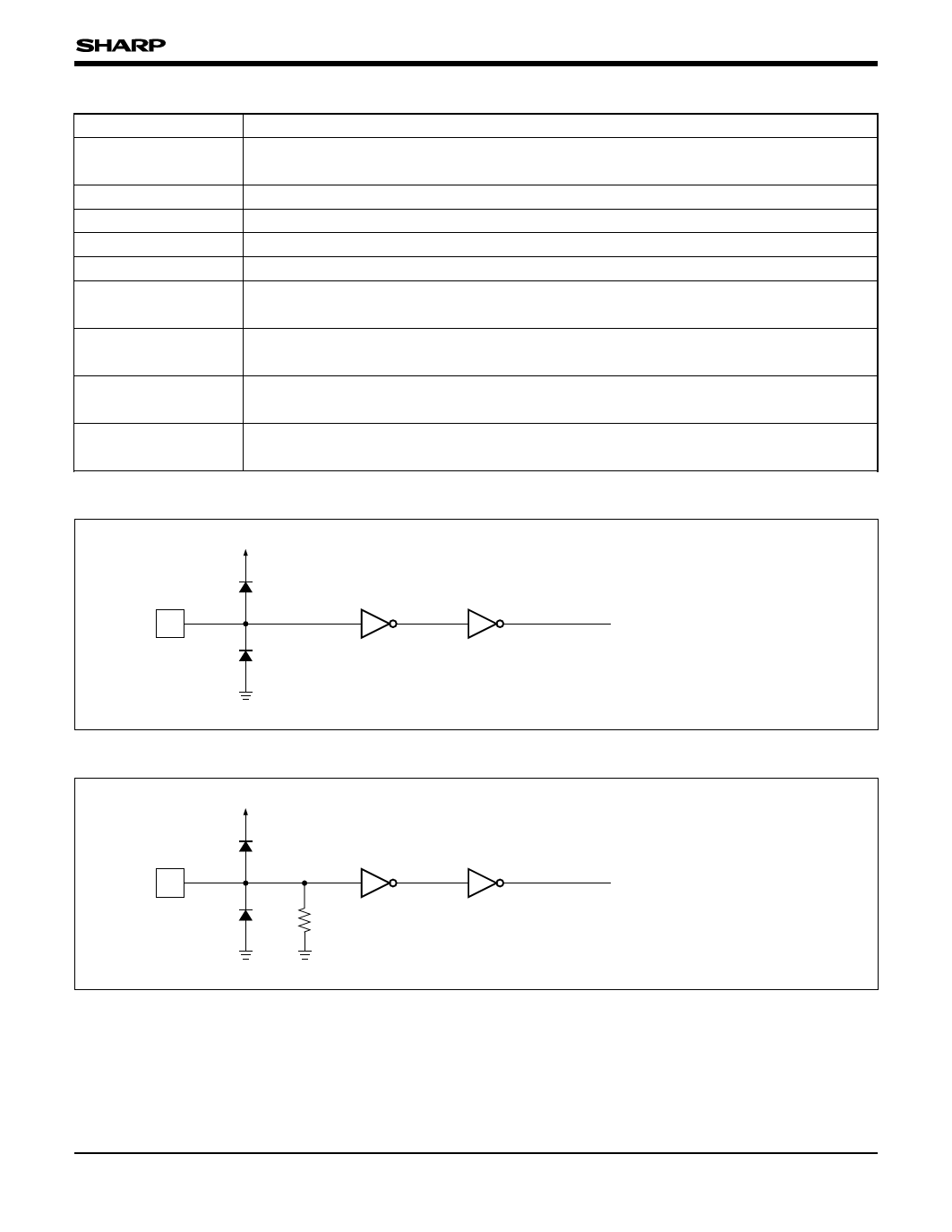
Fig. 1 Input Circuit (1)
To Internal Circuit
¿Applicable pins¡
LBR, LS, REV
VCC
I
To Internal Circuit
GND GND
Fig. 2 Input Circuit (2)
¿Applicable pin¡
POL
4
Share Link: 