LH168M 데이터 시트보기 (PDF) - Sharp Electronics
부품명
상세내역
제조사
LH168M Datasheet PDF : 17 Pages
| |||
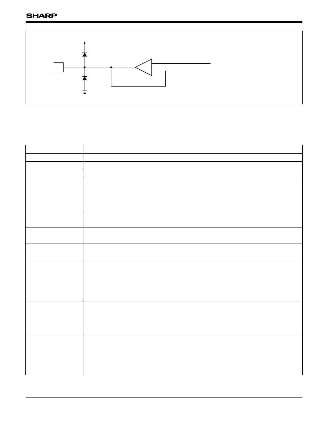
LH168M
VLS
Operational Amplifier
+
O
–
GND
From Internal Circuit
¿Applicable pins¡
XO1-XO128,
YO1-YO128,
ZO1-ZO128
Fig. 5 Output Circuit
FUNCTIONAL DESCRIPTION
Pin Functions
SYMBOL
VCC
VLS
GND
SPIO
SPOI
LBR
LS
CKP
CKN
VH0-VH64
VL0-VL64
X0P-X2N
Y0P-Y2N
Z0P-Z2N
XO1-XO128,
YO1-YO128,
ZO1-ZO128
FUNCTIONS
Used as power supply pin for digital circuit, connected to +3.0 to +3.6 V.
Used as power supply pin for analog circuit, connected to +8.0 to +12.0 V.
Used as ground pin, connected to 0 V.
Used as input pins of start pulse and also used as output pins for cascade connection.
When "H" is input into start pulse input pin, data sampling is started. On completion of
sampling, "H" pulse is output to output pin for cascade connection. Pin functions are
selected by LBR. For selecting, refer to "Functional Operations".
Used as input pin for selecting the shift register direction. For selecting, refer to
"Functional Operations".
Used as input pin for parallel transfer from sampling memory to hold memory. Data is
transferred at the rising edge and output from LCD drive output pin.
Used as shift clock input pin. Data is latched into sampling memory from data input pin at
the falling edge and the rising edge. (Use RSDS input voltage : 0 V to VCC – 1.0 V)
Used as reference voltage input pins. Hold the reference voltage fixed during the period of
LCD drive output. For relation between input data and output voltage values, refer to
"Output Voltage Value". For internal gamma correction, refer to "Gamma Correction
Value". Observe the following relation for input voltage.
VLS > VH0 ≥ VH8 ≥ π ≥ VH64 ≥ VL64 ≥ VL56 ≥ π ≥ VL0 > GND.
Used as data input pins of R, G, and B colors. 3-bit data are input from data pins at the
falling edge and the rising edge of CKP (CKN). For relation between input data and output
voltage values, refer to "Functional Operations" and "Output Voltage Value". Select the
data to be entered into X, Y, and Z according to picture element arrays of the panel.
Used as LCD drive output pins which output the voltage c/orresponding to the input of data
input pins (X0P to X2N, Y0P to Y2N, Z0P to Z2N). Data of XO1 to XO128 correspond to X0P
to X2N. Data of YO1 to YO128 correspond to Y0P to Y2N, and data of ZO1 to ZO128
correspond to Z0P to Z2N. For relation between input data and output voltage values, refer
to "Functional Operations" and "Output Voltage Value".
6
Share Link: 