DTC113TL 데이터 시트보기 (PDF) - Unisonic Technologies
부품명
상세내역
제조사
DTC113TL Datasheet PDF : 3 Pages
| |||
DTC113T
NPN SILICON TRANSISTOR
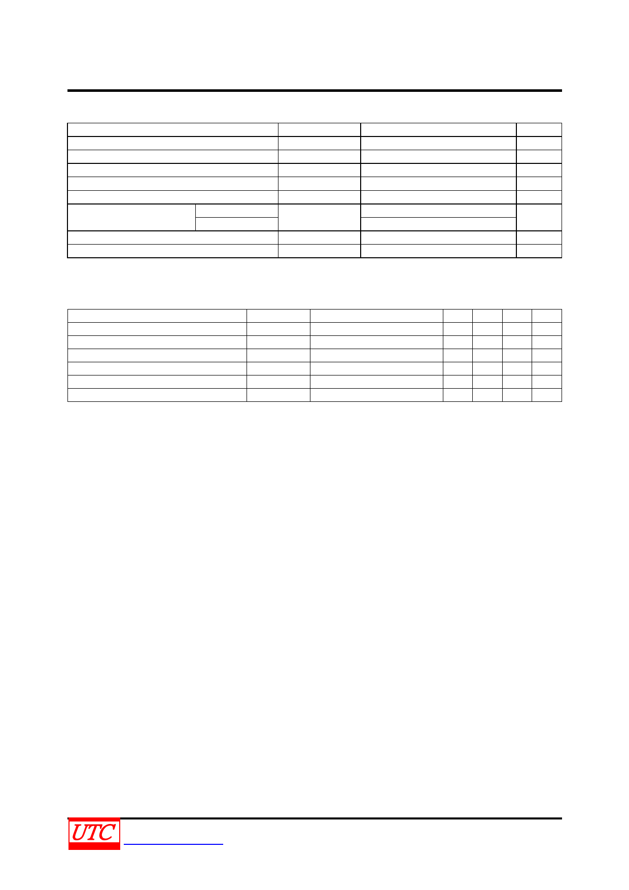
ABSOLUTE MAXIMUM RATINGS (TA=25℃, unless otherwise specified)
PARAMETER
SYMBOL
RATINGS
UNIT
Collector to Base Voltage
VCBO
50
V
Emitter to Base Voltage
VEBO
6
V
Collector to Emitter voltage
VCEO
50
V
Collector Current
IC
100
mA
Peak Collector Current
ICM
200
mA
SOT-23/SOT-323
Collector Power Dissipation
SOT-523
PC
200
mW
150
Junction Temperature
TJ
+150
℃
Storage Temperature
TSTG
-55~+150
℃
Note: Absolute maximum ratings are those values beyond which the device could be permanently damaged.
Absolute maximum ratings are stress ratings only and functional device operation is not implied.
ELECTRICAL CHARACTERISTICS (TA=25℃)
PARAMETER
Collector-Emitter Breakdown Voltage
Collector Cut-off Current
DC Current Gain
Collector-Emitter Saturation Voltage
Input Resistance
Current Gain Bandwidth Product
SYMBOL
BVCEO
ICBO
hFE
VCE(SAT)
R1
fT
TEST CONDITIONS
IC=100μA, RBE=∞
VCB=50V, IE=0
VCE=5V, IC=1mA
IC=10mA, IB=0.5mA
VCE=6V, IE=-10mA
MIN TYP MAX UNIT
50
V
0.1 μA
100
0.3 V
0.7 1.0 1.3 kΩ
200
MHz
UNISONIC TECHNOLOGIES CO., LTD
www.unisonic.com.tw
2 of 3
QW-R223-001.B
Share Link: 