RF2352 데이터 시트보기 (PDF) - RF Micro Devices
부품명
상세내역
제조사
RF2352 Datasheet PDF : 6 Pages
| |||
Preliminary
RF2352
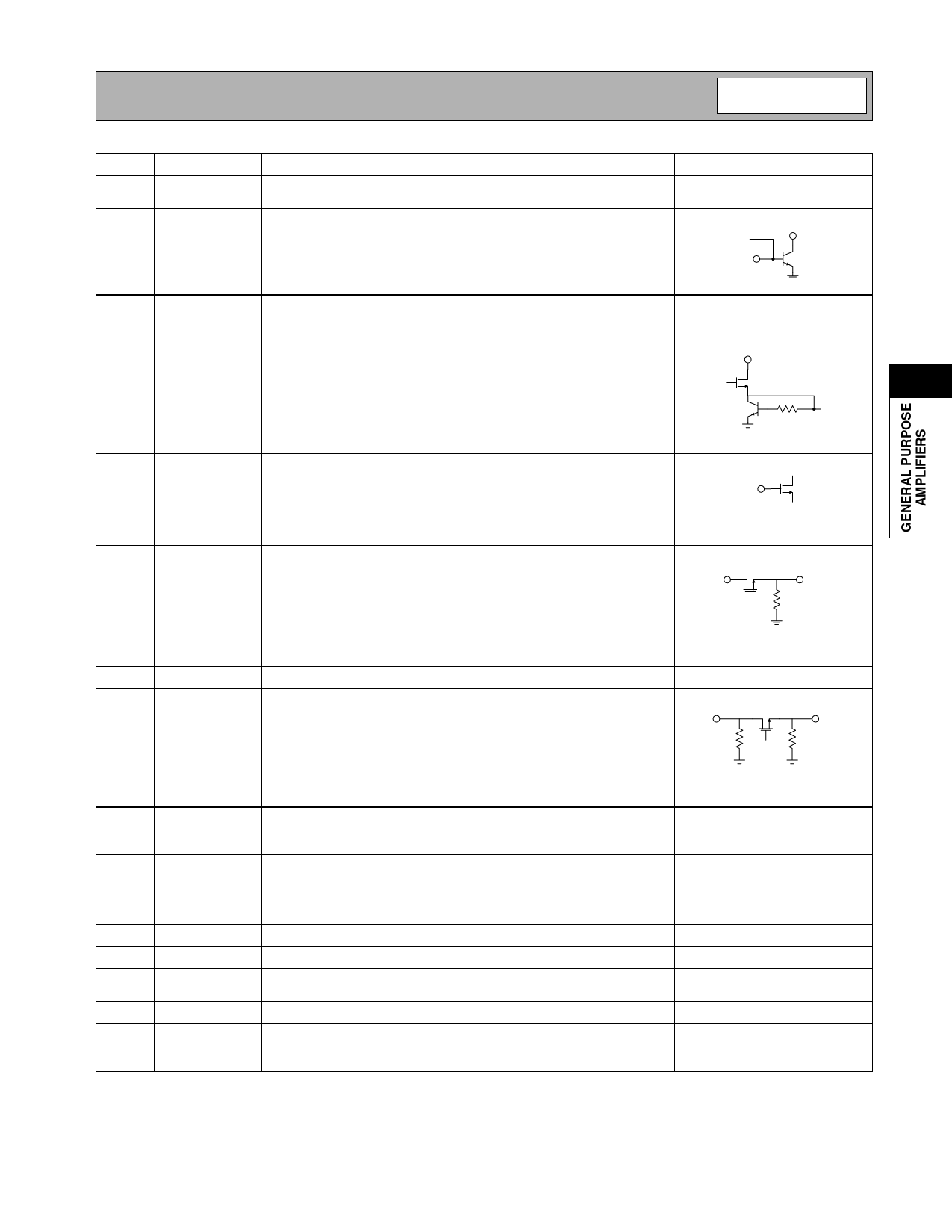
Pin Function Description
Interface Schematic
1
GND
Ground connection. For best performance, keep traces physically short
and connect immediately to ground plane.
2
RF IN
RF input pin. It is DC-coupled and looks like 50Ω from 824MHz to
925 MHz.
RF OUT
Bias
RF IN
3
NC
Not connected.
4
VREF
Provides the bias voltage for controlling the RF amplifier current drain.
This pin is typically connected through a resistor to an external regu-
VREF
lated power supply. It may be connected to the same power supply as
the VCC pin. However, if more bias control is desired, it may be con-
nected to a separate supply. With a series external resistor of 1500Ω
and power supply of 3V applied, the amplifier current drain should be
around 14mA. By increasing the resistor, the amplifier current drain
may be dropped. Conversely, by decreasing the resistor, the amplifier
current may be increased to a maximum of 30mA.
5
PD
Power down function. When 0V to 0.5V is applied, the device is in
Bypass Mode: the amplifier is shut off and the MOSFET switches are
activated. There is no DC current dissipation in this state. When 1.5V to
PD
3V is applied, the device is switched to High Gain Mode: the amplifier is
activated and the MOSFET switches are opened. This is the normal
operating mode.
6
ATT OUT1 Output of the first MOSFET switch. DC-coupled. When the PD pin is
grounded (Bypass Mode), the MOSFET switches are shorted, sending
any signals at the RF IN pin through the first MOSFET and off the chip.
RF IN
In cases where minimum RF attenuation is desired, this pin should be
shorted with 50Ω microstrip to the ATT IN pin. This setup will yield
approximately 4dB of insertion loss. If more attenuation is desired, a
resistive pad between the ATT OUT1 and ATT IN pins can be added to
the PC board.
7
NC
Not connected.
8
ATT IN
Input to the second MOSFET switch. DC-coupled. When the PD pin is
grounded (Bypass Mode), the MOSFET switches are shorted. See the ATT IN
ATT OUT1 pin description for setup options.
4
ATT OUT1
ATT OUT2
9
10
11
12
13
14
15
16
Pkg
Base
GND
ATT OUT2
VCC
RF OUT
NC
NC
RF GND
NC
GND
Ground connection. For best performance, keep traces physically short
and connect immediately to ground plane.
Output of the second MOSFET switch. DC-coupled. When the PD pin
is grounded (Bypass Mode), the MOSFET switches are shorted. This
pin should be shorted with 50Ω microstrip to the amplifier load.
Provides the power supply to the logic circuitry on the IC.
Amplifier output pin. An open collector output that needs VCC applied
to it through an inductor. Typically, a shunt inductor, series capacitor
matching network is used to provide a 50Ω output match.
Not connected.
Not connected.
Amplifier ground. For best performance, keep traces physically short
and connect immediately to ground plane.
Not connected.
Ground connection for die flag. The backside of the package should be
soldered to a top side ground pad which is connected to the ground
plane with multiple vias.
Rev A4 010720
4-179
Share Link: 