RMPA1953-103 데이터 시트보기 (PDF) - Raytheon Company
부품명
상세내역
제조사
RMPA1953-103 Datasheet PDF : 8 Pages
| |||
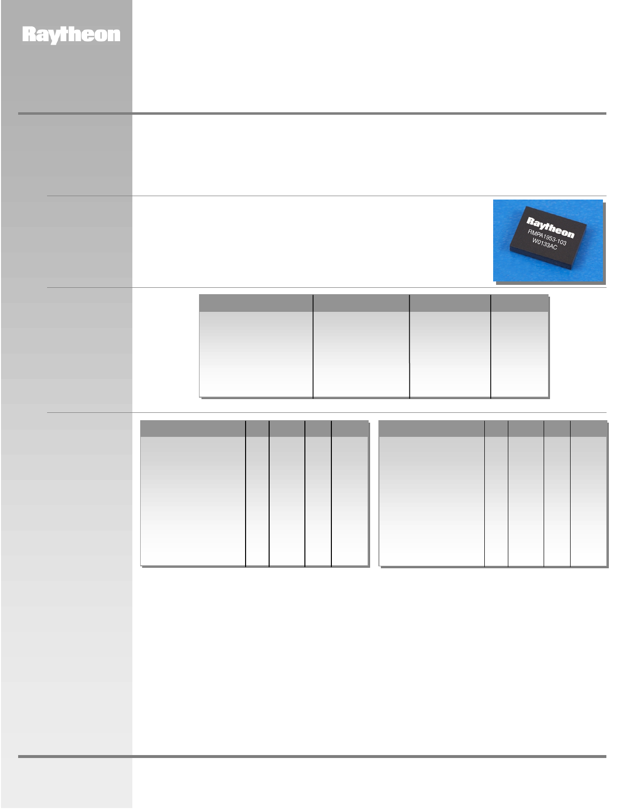
RMPA1953-103
3V PCS CDMA & CDMA2000 Power Amplifier
Module with Digital Bias Control ADVANCED INFORMATION
Description
The RMPA1953-103 is a power amplifier for CDMA and CDMA2000-1X personal communications system (PCS)
applications. The PA is internally matched to 50 ohms to minimize the use of external components. Advanced DC
power management reduces current consumption during peak phone usage at backed-off RF power levels.
Advanced digital bias control reduces the number of interface components to baseband. High power-added
efficiency and excellent linearity are achieved using Raytheon’s InGaP Heterojunction Bipolar Transistor (HBT)
technology.
Features
Single positive-supply operation and power-down mode
Low backed-off power current consumption: 75 mA @ 12 dBm Pout
30% power-added efficiency at +28.5 dBm CDMA average output power
Compact LCC package: 6.0 x 8.0 x 1.5 mm3
50 ohm matched and DC blocked input/output
Advanced Digital Bias Control and DC Power Management
Absolute
Maximum
Ratings1
Parameter
Symbol
Value
Unit
Supply Voltages
Vcc1, Vcc2, and Vbias
5
V
Bias Voltage 1 and 2
Vba1, Vba2
2.5
V
Chip Enable
Venbl
3.0
V
RF Input Power
Pin
+5
dBm
Case Operating Temperature
Tc
-30 to +85
°C
Storage Temperature
Tstg
-55 to +150
°C
Electrical
Characteristics2
Parameter
Operating Frequency
Gain
(Po=12 dBm)
(Po=28.5 dBm)
Linear Output Power
CDMA PAE
(Po=28.5 dBm)
(Po=19 dBm)
ACPR3
ACPR24
Min Typ Max Unit
1850
1910 MHz
22
27 30
28.5
28 dB
34 dB
dBm
30
%
8
%
-47 -51
dBc
-56
dBc
Parameter
Min
Noise Power
(Po ≤ 28.5 dBm)
Input VSWR (50Ω)
Itotal @28.5 dBm Pout
Itotal @12 dBm Pout
Stability (All spurious)5
Harmonics (Po ≤ 28.5 dBm)
2fo, 3fo, 4fo
Power Shutdown Current6
Vcc
3.1
Typ
2.0:1
680
75
<1
3.4
Max Unit
-137
2.5:1
-65
dBm/Hz
mA
mA
dBc
-30 dBc
uA
4.6
V
www.raytheonrf.com
Notes:
1. No permanent damage with only one parameter set at extreme limit. Other parameters set to typical values.
2. All parameters met at Tc =+25°C, Vcc =+3.4V, Vref=+2.9V, f=1880 MHz and load VSWR ≤ 1.2:1.
3. Po ≤ 28.5 dBm at Vcc=3.4V; CDMA Waveform measured using the ratio of average power within a 1.23 MHz channel to average power
within a 30 kHz bandwidth at + 1.25 MHz offset.
4. Po ≤ 28.5 dBm at Vcc=3.4V; CDMA Waveform measured using the ratio of average power within a 1.23 MHz channel to average power
within a 30 kHz bandwidth at +1.98 MHz offset.
5. Output VSWR ≤ 6:1, all phase angles.
6. No applied RF signal. Vcc=+3.4V nominal, Venbl=+0.2V maximum.
Characteristic performance data and specifications are subject to change without notice.
Revised November 14, 2001
Page 1
Raytheon RF Components
362 Lowell Street
Andover, MA 01810
Share Link: 