EL2003 데이터 시트보기 (PDF) - Intersil
부품명
상세내역
제조사
EL2003 Datasheet PDF : 12 Pages
| |||
EL2003, EL2033
Absolute Maximum Ratings (TA = 25°C)
VS Supply Voltage (V+ - V-). . . . . . . . . . . . . . . . . . . ±18V or 36V
VIN Input Voltage . . . . . . . . . . . . . . . . . . . . . . . . . . . .±15V or VS
If the input exceeds the ratings shown (or the supplies) or if the input to output
voltage exceeds ±7.5V then the input current must be limited to ±50 mA. See
the application hints for more information.
IIN Input Current (See note above) . . . . . . . . . . . . . . . . . ±50mA
PD Power Dissipation . . . . . . . . . . . . . . . . . . . . . . . See Curves
The maximum power dissipation depends on package type, ambient
temperature and heat sinking. See the characteristic curves for more details.
Output Short Circuit Duration . . . . . . . . . . . . . . . . . . . . . Continuous
A heat sink is required to keep the junction temperature below the absolute
maximum when the output is short circuited.
TA Operating Temperature Range
EL2003C/EL2033C. . . . . . . . . . . . . . . . . . . . . .-40°C to +85°C
TJ Operating Junction Temperature
Metal Can . . . . . . . . . . . . . . . . . . . . . . . . . . . . . . . . . . . 175°C
Plastic . . . . . . . . . . . . . . . . . . . . . . . . . . . . . . . . . . . . . . 150°C
TST Storage Temperature . . . . . . . . . . . . . . . . . . .-65°C to +150°C
CAUTION: Stresses above those listed in “Absolute Maximum Ratings” may cause permanent damage to the device. This is a stress only rating and operation of the
device at these or any other conditions above those indicated in the operational sections of this specification is not implied.
IMPORTANT NOTE: All parameters having Min/Max specifications are guaranteed. Typical values are for information purposes only. Unless otherwise noted, all tests
are at the specified temperature and are pulsed tests, therefore: TJ = TC = TA
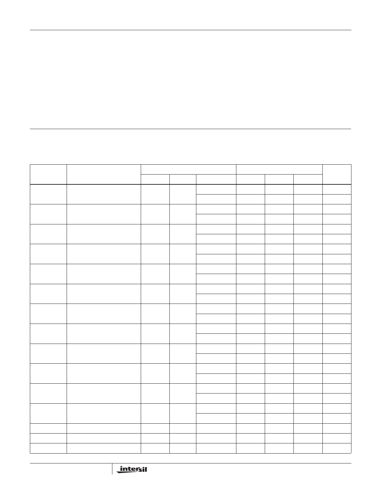
Electrical Specifications VS = ±15V, RS = 50Ω
TEST CONDITIONS
PARAMETER
DESCRIPTION
VOS
Output Offset Voltage
IIN
Input Current
RIN
Input Resistance
AV1
Voltage Gain
AV2
Voltage Gain
AV3
Voltage Gain with VS = ±5V
V01
Output Voltage Swing
V02
Output Voltage Swing
ROUT
Output Resistance
IOUT
Output Current
IS
Supply Current
PSRR
Supply Rejection (Note 2)
SR1
Slew Rate (Note 3)
VIN
0
0
±12V
±12V
±6V
±3V
±14V
±12V
±2V
±12V
0
0
±10V
LOAD
∞
∞
100Ω
1kΩ
50Ω
50Ω
1kΩ
100Ω
50Ω
(Note 1)
∞
∞
1kΩ
TEMP
25°C
TMIN, TMAX
25°C, TMAX
TMIN
25°C, TMAX
TMIN
25°C
TMIN, TMAX
25°C
TMIN, TMAX
25°C
TMIN, TMAX
25°C
TMIN, TMAX
25°C
TMIN, TMAX
25°C
TMIN, TMAX
25°C
TMIN, TMAX
25°C, TMAX
TMIN
25°C
TMIN, TMAX
25°C
SR2
Slew Rate (Note 4)
±5V
50Ω
25°C
THD
Distortion @ 1kHz
4VRMS
50Ω
25°C
MIN
-40
-50
-25
-50
0.5
0.05
0.98
0.97
0.83
0.80
0.82
0.79
±13
±12.5
±10.5
±10
±105
±100
60
50
600
200
LIMITS
TYP
5
-5
2
0.99
0.90
0.89
±13.5
±11.3
7
±230
10
80
1200
400
0.2
MAX
40
50
25
50
10
12
15
20
1
UNIT
mV
mV
µA
µA
MΩ
MΩ
V/V
V/V
V/V
V/V
V/V
V/V
V
V
V
V
Ω
Ω
mA
mA
mA
mA
dB
dB
V/µs
V/µs
%
2
Share Link: 