EL2003 데이터 시트보기 (PDF) - Intersil
부품명
상세내역
제조사
EL2003 Datasheet PDF : 12 Pages
| |||
EL2003, EL2033
Parallel Operation
IOUT ≥ ±300mA
ROUT 2Ω
BW 100MHz
SR = 1000V/µs
J1, J2 2N5911 Dual FET
R1, R2 Offset Adjust
FET INPUT BUFFER WITH HIGH OUTPUT CURRENTS
Resistive Loads
The DC gain of the EL2003 and EL2033 is the product of the
unloaded gain (0.995) and the voltage divider formed by the
device output resistance and the load resistance.
AV = 0.995 × R-----L----+---R--R---L--O----U-----T-
The high frequency response of the EL2003 and EL2033
varies with the value of the load resistance as shown in the
characteristic curves. If the 100MHz peaking is undesirable
when driving load resistors greater than 50Ω, an RC snubber
circuit can be used from the output to ground. The snubber
circuit works by presenting a high frequency load resistance
of less than 50Ω while having no loading effect at low
frequencies.
RL = 100Ω, CL = 10pF, VS = ±15V
Top is VIN, Bottom is VOUT
LARGE SIGNAL RESPONSE
Capacitive Loads
The EL2003 and EL2033 are stable driving any type of
capacitive load. However, when driving a pure capacitance
of less than a thousand picofarads the frequency response
has excessive peaking as shown in the characteristic curves.
The squarewave response will have large overshoots and
will ring for several hundred nanoseconds.
If the peaking and ringing cause system problems they can
be eliminated with an RC snubber circuit from the output to
ground. The values can be found empirically by observing a
squarewave or the frequency response. First just put the
resistor alone from output to ground until the desired
response is obtained. Of course the gain will be reduced due
to ROUT. Then put capacitance in series with the resistor to
restore the gain at low frequencies. Start with a small
capacitor and increase until the response is optimum. Too
large a capacitor will roll the gain off prematurely and result
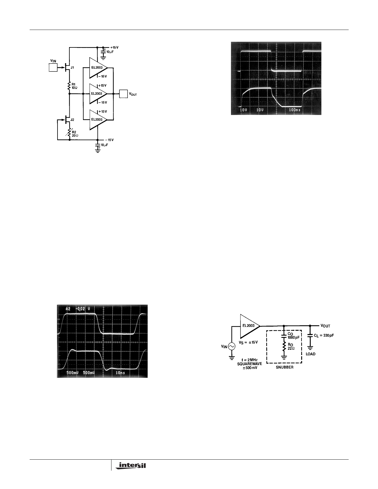
in a longer settling time. The figure below shows an example
of an EL2003 driving a 330pF load, which is similar to the
input of a flash converter.
RL = 50Ω, CL = 10pF, VS = ±15V
Top is VIN, Bottom is VOUT
SMALL SIGNAL RESPONSE
6
Share Link: 