EL2150 데이터 시트보기 (PDF) - Intersil
부품명
상세내역
제조사
EL2150 Datasheet PDF : 19 Pages
| |||
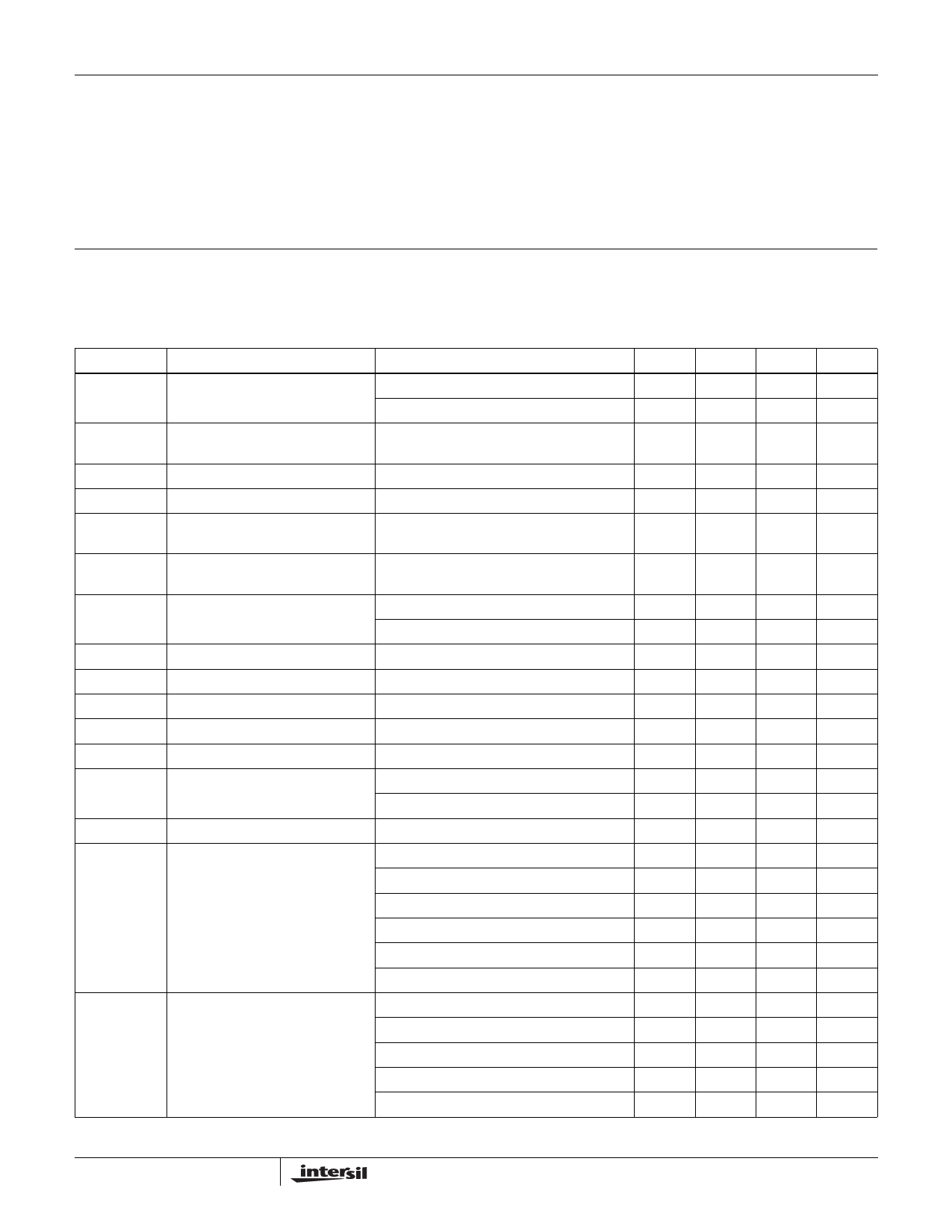
EL2150, EL2157
Absolute Maximum Ratings (TA = 25°C)
Supply Voltage between VS+ and GND . . . . . . . . . . . . . . . . +12.6V
Input Voltage (IN+, IN-, ENABLE, CLAMP) . . . GND-0.3V, VS+0.3V
Differential Input Voltage . . . . . . . . . . . . . . . . . . . . . . . . . . . . . . .±6V
Maximum Output Current. . . . . . . . . . . . . . . . . . . . . . . . . . . . . 90mA
Output Short Circuit Duration. . . . . . . . . . . . . . . . . . . . . . . . (Note 1)
Power Dissipation . . . . . . . . . . . . . . . . . . . . . . . . . . . . . See Curves
Storage Temperature Range . . . . . . . . . . . . . . . . . .-65°C to +150°C
Ambient Operating Temperature Range . . . . . . . . . .-40°C to +85°C
Operating Junction Temperature . . . . . . . . . . . . . . . . . . . . . . . 150°C
CAUTION: Stresses above those listed in “Absolute Maximum Ratings” may cause permanent damage to the device. This is a stress only rating and operation of the
device at these or any other conditions above those indicated in the operational sections of this specification is not implied.
IMPORTANT NOTE: All parameters having Min/Max specifications are guaranteed. Typical values are for information purposes only. Unless otherwise noted, all tests
are at the specified temperature and are pulsed tests, therefore: TJ = TC = TA
DC Electrical Specifications VS = +5V, GND = 0V, TA = 25°C, VCM = 1.5V, VOUT = 1.5V, VCLAMP = +5V, VENABLE = +5V, unless
otherwise specified. (Note 1)
PARAMETER
DESCRIPTION
CONDITIONS
MIN
TYP
MAX
UNIT
VOS
Offset Voltage
SO package
SOT-23 package
-2
2
mV
-3
3
mV
TCVOS
Offset Voltage Temperature
Coefficient
Measured from TMIN to TMAX
10
µV/°C
IB
IOS
TCIOS
Input Bias Current
Input Offset Current
Input Bias Current Temperature
Coefficient
VIN = 0V
VIN = 0V
Measured from TMIN to TMAX
-5.5
-10
µA
-750
150
750
nA
50
nA/°C
PSRR
Power Supply Rejection Ratio
VS = VENABLE = 2.7V to 12V, VCLAMP =
55
70
dB
OPEN
CMRR
CMIR
RIN
CIN
ROUT
IS,ON
IS,OFF
PSOR
Common Mode Rejection Ratio
Common Mode Input Range
Input Resistance
Input Capacitance
Output Resistance
Supply Current - Enabled
Supply Current - Shut Down
Power Supply Operating Range
VCM = 0V to 3.8V
VCM = 0V to 3.0V
Common mode
SO package
AV = 1
VS = VCLAMP = 12V, VENABLE = 12V
VS = VCLAMP = 10V, VENABLE = 0.5V
VS = VCLAMP = 12V, VENABLE = 0.5V
55
65
dB
55
70
dB
0
VS-1.2
V
1
2
MΩ
1
pF
40
mΩ
5
6.5
mA
0
50
µA
5
µA
2.7
12.0
V
AVOL
Open Loop Gain
VS = VCLAMP = 12V, VOUT = 2V
65
80
dB
9V, RL = 1kΩ to GND
VOUT = 1.5V to 3.5V
70
dB
RL = 1kΩ to GND
VOUT = 1.5V to 3.5V
60
dB
RL = 150Ω to GND
VOP
Positive Output Voltage Swing
VS = 12V, AV = 1, RL= 1kΩ to 0V
10.8
V
VS = 12V, AV = 1, RL = 150Ω to 0V
9.6
10.0
V
VS = ±5V, AV = 1, RL = 1kΩ to 0V
4.0
V
VS = ±5V, AV = 1, RL = 150Ω to 0V
3.4
3.8
V
VS = 3V, AV = 1, RL = 150Ω to 0V
1.8
1.95
V
3
Share Link: 