EL4452CN 데이터 시트보기 (PDF) - Elantec -> Intersil
부품명
상세내역
제조사
EL4452CN Datasheet PDF : 12 Pages
| |||
EL4452C
Wideband Variable-Gain Amplifier with Gain of 10
Applications Information Contd
and outputs will have to have their levels shifted
above ground to accommodate the lack of nega-
tive supply
The power dissipation of the EL4452 increases
with power supply voltage and this must be
compatible with the package chosen This is a
close estimate for the dissipation of a circuit
PDe2cVScIS maxa(VSbVO)cVO RPAR
where IS max is the maximum supply current
VS is the g supply voltage (assumed
equal)
VO is the output voltage
RPAR is the parallel of all resistors loading
the output
For instance the EL4452 draws a maximum of
x 18mA With light loading RPAR % and the
dissipation with g5V supplies is 180 mW The
maximum supply voltage that the device can run
on for a given PD and other parameters is
VS maxe(PDaVO2 RPAR) (2ISaVO RPAR)
The maximum dissipation a package can offer is
PD max e (TJ maxbTA max) iJA
Where TJ max is the maximum die tempera-
ture 150 C for reliability less to re-
tain optimum electrical performance
TA max is the ambient temperature
70 C for commercial and 85 C for in-
dustrial range
iJA is the thermal resistance of the
mounted package obtained from
data sheet dissipation curves
The more difficult case is the SO-14 package
With a maximum die temperature of 150 C and a
maximum ambient temperature of 85 C the 65 C
temperature rise and package thermal resistance
of 120 C W gives a dissipation of 542 mW at
85 C This allows the full maximum operating
supply voltage unloaded but reduced if loaded
Output Loading
The output stage of the EL4452 is very powerful
It can typically source 80 mA and sink 120 mA
Of course this is too much current to sustain and
the part will eventually be destroyed by excessive
dissipation or by metal traces on the die opening
The metal traces are completely reliable while de-
livering the 30 mA continuous output given in
the Absolute Maximum Ratings table in this
data sheet or higher purely transient currents
Gain changes only 0 2% from no load to a 100X
load Heavy resistive loading will degrade fre-
quency response and distortion for loads k100X
Capacitive loads will cause peaking in the fre-
quency response If capacitive loads must be driv-
en a small-valued series resistor can be used to
isolate it 12X to 51X should suffice A 22X series
resistor will limit peaking to 1 dB with even a
220 pF load
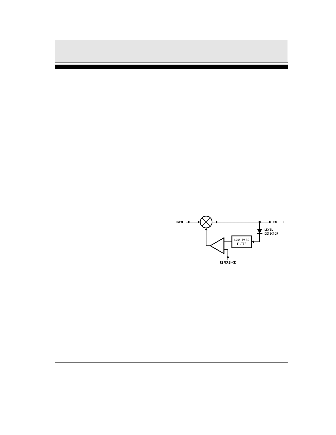
AGC Circuits
The basic AGC (automatic gain control) loop is
this
Basic AGC Loop
4452 – 24
A multiplier scales the input signal and provides
necessary gain and buffers the signal presented
to the output load a level detector (shown sche-
matically here as a diode) converts some measure
of the output signal amplitude to a DC level a
low-pass filter attenuates any signal ripple pres-
ent on that DC level and an amplifier compares
that level to a reference and amplifies the error to
create a gain-control voltage for the multiplier
The circuitry is a servo that attempts to keep the
output amplitude constant by continuously ad-
justing the multiplier’s gain control input
9
Share Link: 