EL5120TIWTZ-T7 데이터 시트보기 (PDF) - Intersil
부품명
상세내역
제조사
EL5120TIWTZ-T7 Datasheet PDF : 14 Pages
| |||
EL5120T
Absolute Maximum Ratings (TA = +25°C)
Supply Voltage between VS+ and VS-. . . . . . . . . . . . . . . . . . . . . . . . . +19.8V
Input Voltage Range (VIN+, VIN-). . . . . . . . . . . . . . . . . . . . . VS- - 0.5V, VS+ + 0.5V
Input Differential Voltage (VIN+ - VIN-) . . . . . . . . . . . . . . . . . . . . . . . . . . . . . . .
. . . . . . . . . . . . . . . . . . . . . . . . . . . . . . . . . . . . . . . . (VS+ + 0.5V)-(VS- - 0.5V)
Maximum Continuous Output Current . . . . . . . . . . . . . . . . . . . . . . . ±70mA
ESD Rating
Human Body Model (Tested per JESD22-A114) . . . . . . . . . . . . . . . 4000V
Machine Model (Tested per JESD22-A115). . . . . . . . . . . . . . . . . . . . 300V
Charged Device Model (Tested per JESD22-C101). . . . . . . . . . . . . 2000V
Latch Up (Tested per JESD78; Class II, Level A) . . . . . . . . . . . . . . . . 100mA
Thermal Information
Thermal Resistance (Typical)
5 Ld TSOT (Notes 4, 5)
θJA (°C/W) θJC (°C/W)
215
290
Storage Temperature . . . . . . . . . . . . . . . . . . . . . . . . . . . . . .-65°C to +150°C
Ambient Operating Temperature . . . . . . . . . . . . . . . . . . . . . -40°C to +85°C
Maximum Junction Temperature . . . . . . . . . . . . . . . . . . . . . . . . . . . .+150°C
Power Dissipation. . . . . . . . . . . . . . . . . . . . . . . . . . . . See Figures 30 and 31
CAUTION: Do not operate at or near the maximum ratings listed for extended periods of time. Exposure to such conditions may adversely impact product
reliability and result in failures not covered by warranty.
NOTES:
4. θJA is measured with the component mounted on a high effective thermal conductivity test board in free air. See Tech Brief TB379 for details.
5. For θJC, the “case temp” location is taken at the package top center.
IMPORTANT NOTE: All parameters having Min/Max specifications are guaranteed. Typ values are for information purposes only. Unless otherwise noted, all tests are
at the specified temperature and are pulsed tests, therefore: TJ = TC = TA
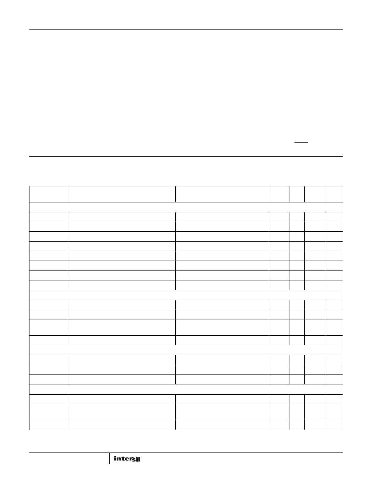
Electrical Specifications VS+ = +5V, VS- = -5V, RL = 10kΩ to 0V, TA = +25°C, unless otherwise specified.
PARAMETER
DESCRIPTION
CONDITIONS
MIN
MAX
(Note 9) TYP (Note 9) UNIT
INPUT CHARACTERISTICS
VOS
TCVOS
IB
RIN
CIN
CMIR
Input Offset Voltage
Average Offset Voltage Drift (Note 6)
Input Bias Current
Input Impedance
Input Capacitance
Common-Mode Input Range
VCM = 0V
VCM = 0V
5
18
mV
5
µV/°C
2
50
nA
1
GΩ
2
pF
-5.5
+5.5
V
CMRR
Common-Mode Rejection Ratio
AVOL
Open Loop Gain
OUTPUT CHARACTERISTICS
For VIN from -5.5V to +5.5V
-4.5V ≤ VOUT ≤ +4.5V
50 75
dB
75 105
dB
VOL
Output Swing Low
VOH
Output Swing High
ISC
Short Circuit Current
IOUT
Output Current
POWER SUPPLY PERFORMANCE
IL = -5mA
IL = +5mA
VCM = 0V, Source: VOUT short to VS-,
Sink: VOUT short to VS+
-4.94 -4.85 V
4.85 4.94
V
±200
mA
±70
mA
(VS+) - (VS-)
IS
PSRR
Supply Voltage Range
Supply Current
Power Supply Rejection Ratio
VCM = 0V, No load
Supply is moved from ±2.25V to ±9.5V
4.5
19
V
750 950 µA
60 75
dB
DYNAMIC PERFORMANCE
SR
Slew Rate (Note 7)
tS
Settling to +0.1% (Note 8)
BW
-3dB Bandwidth
-4.0V ≤ VOUT ≤ +4.0V, 20% to 80%
AV = +1, VOUT = 2V step,
RL = 10kΩ, CL = 8pF
RL = 10kΩ, CL = 8pF
12
V/µs
500
ns
12
MHz
3
FN6895.0
September 27, 2012
Share Link: 