EL5129 데이터 시트보기 (PDF) - Intersil
부품명
상세내역
제조사
EL5129 Datasheet PDF : 13 Pages
| |||
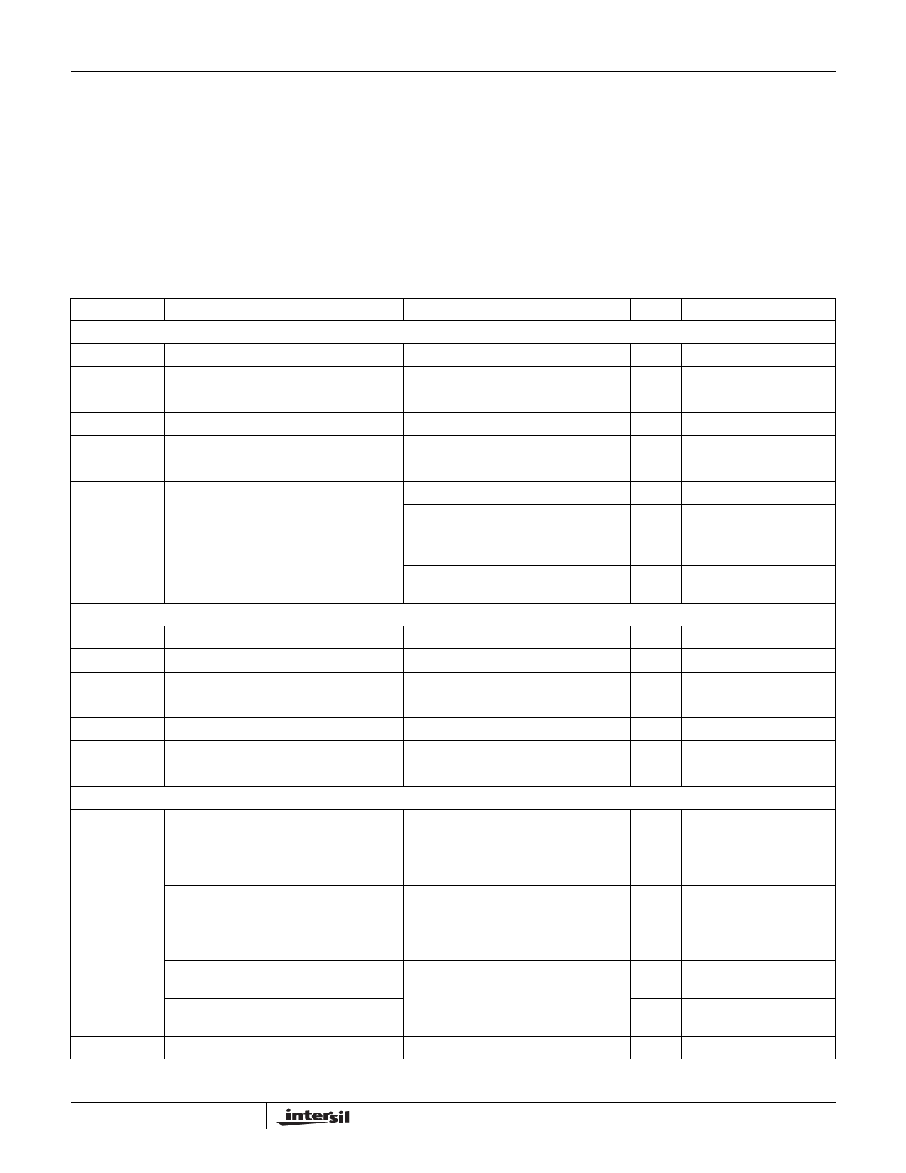
EL5129, EL5329
Absolute Maximum Ratings (TA = 25°C)
Supply Voltage between VS+ and VS- . . . . . . . . . . . . . . . . . . . .+18V
Input Voltage . . . . . . . . . . . . . . . . . . . . . . . . . . VS- -0.5V, VS+ +0.5V
Maximum Continuous Output Current (VOUT0-9) . . . . . . . . . . 15mA
Maximum Continuous Output Current (VOUTA). . . . . . . . . . . 100mA
Power Dissipation . . . . . . . . . . . . . . . . . . . . . . . . . . . . . See Curves
Maximum Die Temperature . . . . . . . . . . . . . . . . . . . . . . . . . . +125°C
Storage Temperature . . . . . . . . . . . . . . . . . . . . . . . .-65°C to +150°C
Ambient Operating Temperature . . . . . . . . . . . . . . . .-40°C to +85°C
CAUTION: Stresses above those listed in “Absolute Maximum Ratings” may cause permanent damage to the device. This is a stress only rating and operation of the
device at these or any other conditions above those indicated in the operational sections of this specification is not implied.
NOTE: All parameters having Min/Max specifications are guaranteed. Typ values are for information purposes only. Unless otherwise noted, all tests
are at the specified temperature and are pulsed tests, therefore: TJ = TC = TA
Electrical Specifications VS+ = +15V, VS- = 0, RL = 10kΩ, CL = 10pF to 0V, TA = 25°C unless otherwise specified
PARAMETER
DESCRIPTION
CONDITIONS
MIN TYP MAX UNIT
INPUT CHARACTERISTICS (REFERENCE BUFFERS)
VOS
TCVOS
IB
RIN
CIN
AV
CMIR
Input Offset Voltage
Average Offset Voltage Drift
Input Bias Current
Input Impedance
Input Capacitance
Voltage Gain
Input Voltage Range
VCM = 0V
(Note 1)
VCM = 0V
1V ≤ VOUT ≤ 14V
EL5129, IN1 to IN3
EL5329, IN1 to IN5
EL5129, IN4 to IN6
2
20
mV
5
µV/°C
2
50
nA
10
MΩ
1.35
pF
0.992
1.008 V/V
1.5
VS+
V
1.5
VS+
V
0
VS+
V
-1.5
EL5329, IN6 to IN10
0
VS+
V
-1.5
INPUT CHARACTERISTICS (VCOM BUFFER)
VOS
Input Offset Voltage
TCVOS
Average Offset Voltage Drift
IB
Input Bias Current
RIN
Input Impedance
CIN
Input Capacitance
VREG
Load Regulation
CMIRCOM
Input Voltage Range VCOM
OUTPUT CHARACTERISTICS (REFERENCE BUFFERS)
VCM = 7.5V
(Note 1)
VCM = 7.5V
VCOM = 7.5V, -60mA < IL < 60mA
1
20
mV
3
µV/°C
2
50
nA
10
MΩ
1.35
pF
-20
+20
mV
0
VS+
V
VOH
High Output Voltage - EL5129 & EL5329
(Output 1)
VIN = 15V, IO = 5mA
14.85 14.9
V
High Output Voltage - EL5129 (Output 2, 3),
EL5329 (Output 2-5)
14.8 14.85
V
High Output Voltage - EL5129 (Output 4-6), VIN = 13.5V, IO = 5mA
EL5329 (Output 6-10)
13.45 13.5
V
VOL
Low Output Voltage - EL5129 (Output 1-3), VIN = 1.5V, IO = 5mA
EL5329 (Output 1-5)
1.5
1.55
V
Low Output Voltage - EL5129 (Output 4-5), VIN = 0V, IO = 5mA
EL5329 (Output 6-9)
150
200
mV
Low Output Voltage - EL5129 (Output 6),
EL5329 (Output 10)
100
150
mV
ISC
Short Circuit Current
100
120
mA
3
FN7430.1
May 13, 2005
Share Link: 