EL5130 데이터 시트보기 (PDF) - Intersil
부품명
상세내역
제조사
EL5130 Datasheet PDF : 12 Pages
| |||
EL5130, EL5131
Absolute Maximum Ratings (TA = +25°C)
Slewrate between VS+ and VS- . . . . . . . . . . . . . . . . . . . . . . . . 1V/µs
Supply Voltage from VS+ to VS- . . . . . . . . . . . . . . . . . . . . . . . 13.2V
IIN-, IIN+, CE . . . . . . . . . . . . . . . . . . . . . . . . . . . . . . . . . . . . . . ±5mA
Continuous Output Current . . . . . . . . . . . . . . . . . . . . . . . . . . 100mA
Thermal Information
Storage Temperature . . . . . . . . . . . . . . . . . . . . . . . .-65°C to +125°C
Ambient Operating Temperature . . . . . . . . . . . . . . . .-40°C to +85°C
Operating Junction Temperature . . . . . . . . . . . . . . . . . . . . . . +125°C
Power Dissipation . . . . . . . . . . . . . . . . . . . . . . . . . . . . . See Curves
Pb-free reflow profile . . . . . . . . . . . . . . . . . . . . . . . . . .see link below
http://www.intersil.com/pbfree/Pb-FreeReflow.asp
CAUTION: Stresses above those listed in “Absolute Maximum Ratings” may cause permanent damage to the device. This is a stress only rating and operation of the
device at these or any other conditions above those indicated in the operational sections of this specification is not implied.
IMPORTANT NOTE: All parameters having Min/Max specifications are guaranteed. Typical values are for information purposes only. Unless otherwise noted, all tests
are at the specified temperature and are pulsed tests, therefore: TJ = TC = TA
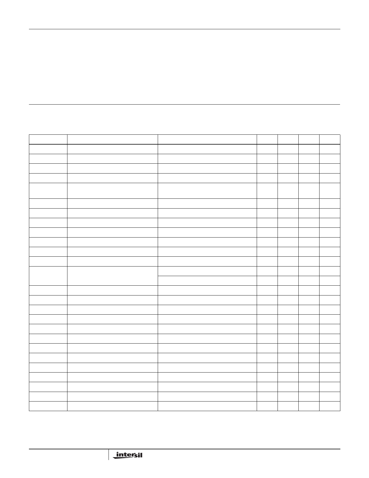
Electrical Specifications VS+ = +5V, VS- = -5V, RL = 500Ω, RG = 50Ω, CL = 5pF, TA = +25°C, Unless Otherwise Specified.
PARAMETER
DESCRIPTION
CONDITIONS
MIN TYP MAX
VOS
TCVOS
IB
IOS
TCIOS
Offset Voltage
Offset Voltage Temperature Coefficient
Input Bias Current
Input Offset Current
Input Bias Current Temperature
Coefficient
Measured from TMIN to TMAX
VIN = 0V
VIN = 0V
Measured from TMIN to TMAX
-0.9
0.2
0.9
0.8
1.5
2.27
3.3
-500
100
500
-3
PSRR
CMRR
CMIR
Power Supply Rejection Ratio
Common Mode Rejection Ratio
Common Mode Input Range
VS = ±4.75V to ±5.25V
VIN = ±3.0V
Guaranteed by CMRR test
75
90
95
110
±3
±3.3
RIN
CIN
IS
AVOL
VO
ISC
BW
BW
GBWP
Input Resistance
Input Capacitance
Supply Current
Open Loop Gain
Output Voltage Swing
Short Circuit Current
-3dB Bandwidth
±0.1dB Bandwidth
Gain Bandwidth Product
Common mode
VOUT = ±2.5V, RL = 1kΩ to GND
RL = 1kΩ, RF = 900Ω, RG = 100Ω
RL = 150Ω
RL = 10Ω
AV = +5, RL = 500Ω
AV = +5, RL = 500Ω
5
20
1
3.0
3.54
4.1
10
16
±3.5 ±3.8
±3.5 ±3.3
50
100
300
60
1500
PM
SR
tR, tF
tPD
tS
dG
dP
eN
iN
Phase Margin
Slew Rate
Rise Time, Fall Time
Propagation Delay
0.01% Settling Time
Differential Gain
Differential Phase
Input Noise Voltage
Input Noise Current
RL = 1kΩ, CL = 6pF
VS = ±5V, RL = 150Ω, VOUT = ±2.5V
±0.1VSTEP
±0.1VSTEP
AV = +2, RF = 1kΩ
AV = +2, RF = 1kΩ
f = 10kHz
f = 10kHz
55
225
350
TBD
TBD
14
0.01
0.01
1.8
1.1
UNIT
mV
µV/°C
µA
nA
nA/°C
dB
dB
V
MΩ
pF
mA
kV/V
V
V
mA
MHz
MHz
MHz
°
V/µs
ns
ns
ns
%
°
nV/√Hz
pA/√Hz
2
FN7381.4
May 4, 2007
Share Link: 