EL5177(2005) 데이터 시트보기 (PDF) - Intersil
부품명
상세내역
제조사
EL5177 Datasheet PDF : 11 Pages
| |||
EL5177
Absolute Maximum Ratings (TA = 25°C)
Supply Voltage (VS+ to VS-) . . . . . . . . . . . . . . . . . . . . . . . . . . . .12V
Maximum Output Current. . . . . . . . . . . . . . . . . . . . . . . . . . . . ±60mA
Storage Temperature Range . . . . . . . . . . . . . . . . . .-65°C to +150°C
Operating Junction Temperature . . . . . . . . . . . . . . . . . . . . . . +135°C
Recommended Operating Temperature . . . . . . . . . .-40°C to +85°C
VIN, VINB, VREF . . . . . . . . . . VS- + 0.8V (min) to VS+ - 0.8V (max)
VIN - VINB . . . . . . . . . . . . . . . . . . . . . . . . . . . . . . . . . . . . . . . . . .±5V
CAUTION: Stresses above those listed in “Absolute Maximum Ratings” may cause permanent damage to the device. This is a stress only rating and operation of the
device at these or any other conditions above those indicated in the operational sections of this specification is not implied.
IMPORTANT NOTE: All parameters having Min/Max specifications are guaranteed. Typ values are for information purposes only. Unless otherwise noted, all tests are
at the specified temperature and are pulsed tests, therefore: TJ = TC = TA
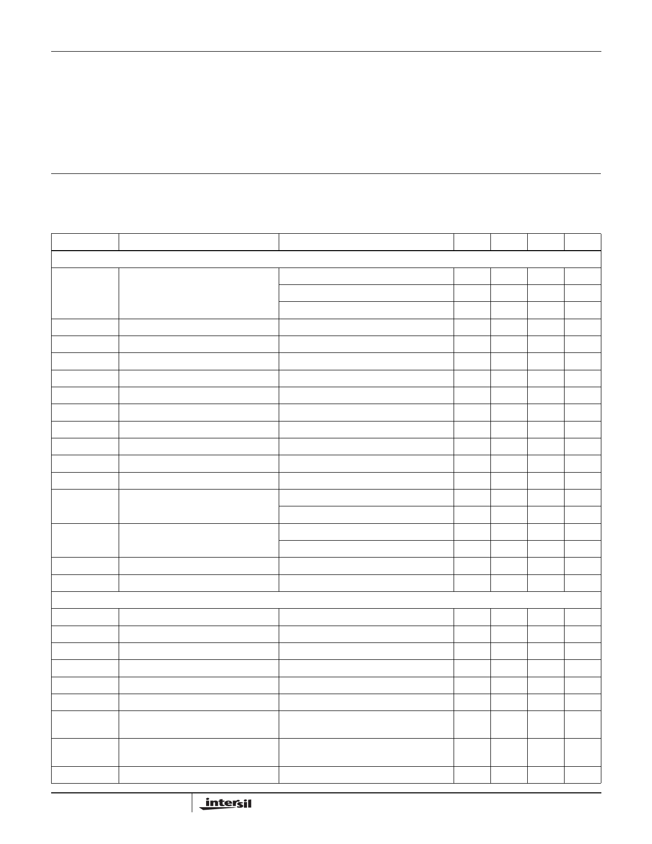
Electrical Specifications VS+ = +5V, VS- = -5V, TA = 25°C, VIN = 0V, RLD = 1kΩ, RF = 0, RG = OPEN, CLD = 2.7pF, unless otherwise
specified.
PARAMETER
DESCRIPTION
CONDITIONS
MIN TYP MAX UNIT
AC PERFORMANCE
BW
BW
SR
TSTL
TOVR
GBWP
-3dB Bandwidth
±0.1dB Bandwidth
Slew Rate
Settling Time to 0.1%
Output Overdrive Recovery Time
Gain Bandwidth Product
AV = 1, CLD = 2.7pF
AV = 2, RF = 500, CLD = 2.7pF
AV = 10, RF = 500, CLD = 2.7pF
AV = 1, CLD = 2.7pF
VOUT = 3VP-P, 20% to 80%
VOUT = 2VP-P
550
130
20
120
800 1100
10
20
200
MHz
MHz
MHz
MHz
V/µs
ns
ns
MHz
VREFBW (-3dB) VREF -3dB Bandwidth
VREFSR+
VREF Slew Rate - Rise
VREFSR-
VREF Slew Rate - Fall
VN
Input Voltage Noise
IN
Input Current Noise
HD2
Second Harmonic Distortion
HD3
Third Harmonic Distortion
dG
Differential Gain at 3.58MHz
dθ
Differential Phase at 3.58MHz
INPUT CHARACTERISTICS
AV =1, CLD = 2.7pF
VOUT = 2VP-P, 20% to 80%
VOUT = 2VP-P, 20% to 80%
at 10kHz
at 10kHz
VOUT = 2VP-P, 5MHz
VOUT = 2VP-P, 20MHz
VOUT = 2VP-P, 5MHz
VOUT = 2VP-P, 20MHz
RLD = 300Ω, AV =2
RLD = 300Ω, AV =2
110
MHz
134
V/µs
70
V/µs
21
nV/√Hz
2.7
pA/√Hz
-95
dBc
-94
dBc
-88
dBc
-87
dBc
0.06
%
0.13
°
VOS
IIN
IREF
RIN
CIN
DMIR
Input Referred Offset Voltage
Input Bias Current (VIN+, VIN-)
Input Bias Current (VREF)
Differential Input Resistance
Differential Input Capacitance
Differential Mode Input Range
±1.4 ±25
mV
-30
-14
-7
µA
0.5
2.3
4
µA
150
kΩ
1
pF
±2.1 ±2.3 ±2.5
V
CMIR+
CMIR-
VREFIN+
Common Mode Positive Input Range at
VIN+, VIN-
Common Mode Negative Input Range at
VIN+, VIN-
Positive Reference Input Voltage Range VIN+ = VIN- = 0V
3.4
V
-4.3
V
3.4
3.7
V
2
FN7344.3
August 8, 2005
Share Link: 