EL5411T(2010) 데이터 시트보기 (PDF) - Intersil
부품명
상세내역
제조사
EL5411T Datasheet PDF : 16 Pages
| |||
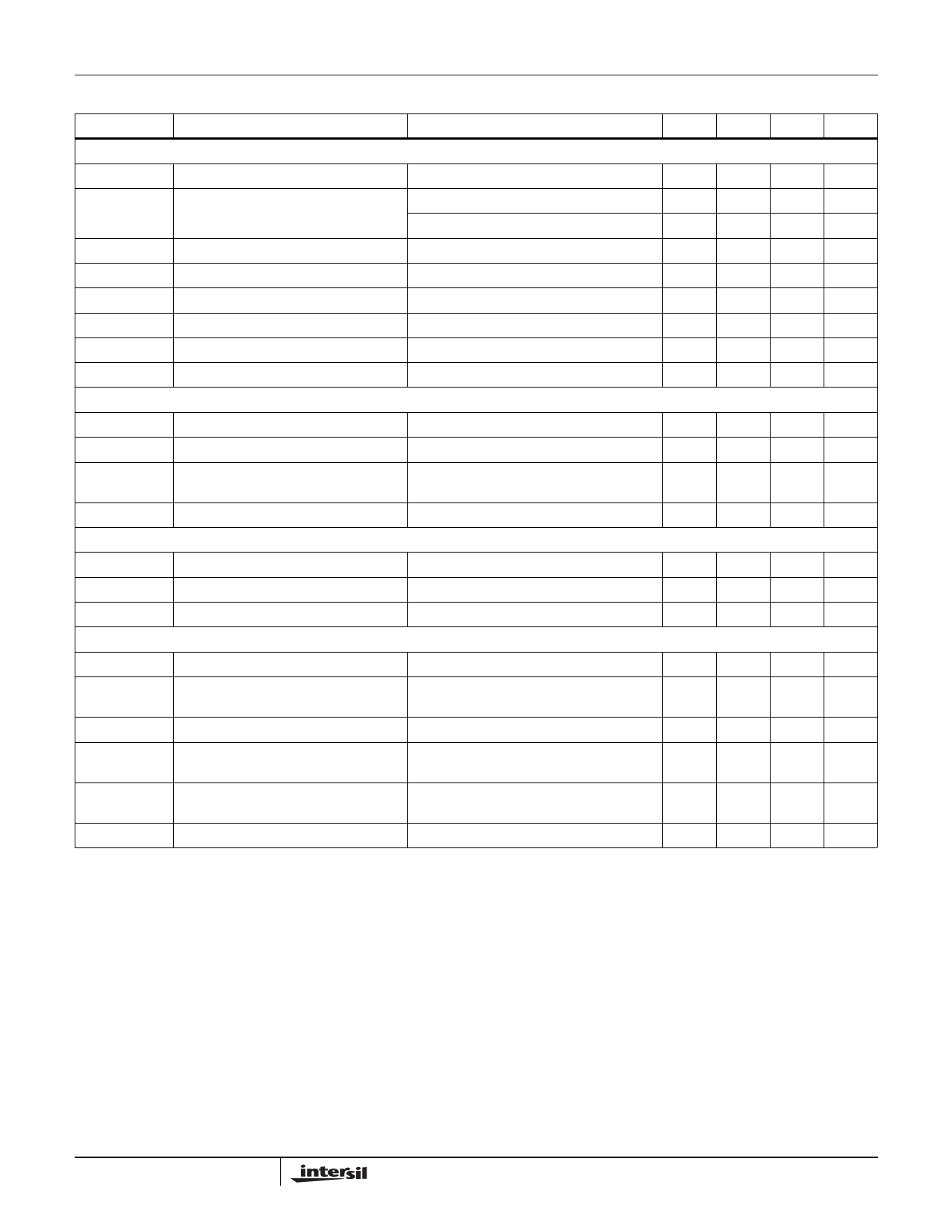
EL5411T
Electrical Specifications VS+ = +18V, VS- = 0V, RL = 1kΩ to 9V, TA = +25°C, Unless Otherwise Specified.
PARAMETER
DESCRIPTION
CONDITION
MIN TYP MAX
UNIT
INPUT CHARACTERISTICS
VOS
TCVOS
Input Offset Voltage
Average Offset Voltage Drift
(Note 6)
VCM = 9V
14 LD HTSSOP package
16 LD TQFN package
3.5
17
mV
21
µV/°C
5
µV/°C
IB
RIN
CIN
CMIR
Input Bias Current
Input Impedance
Input Capacitance
Common-Mode Input Range
VCM = 9V
-0.5
2
60
nA
1
GΩ
2
pF
+18.5 V
CMRR
Common-Mode Rejection Ratio
AVOL
Open-Loop Gain
OUTPUT CHARACTERISTICS
For VIN from -0.5V to 18.5V
0.5V ≤ VOUTx ≤ 17.5V
53
75
dB
62
104
dB
VOL
VOH
ISC
Output Swing Low
Output Swing High
Short-circuit Current
IOUT
Output Current
POWER SUPPLY PERFORMANCE
IL = -6mA
80
150
mV
IL = +6mA
17.85 17.92
V
VCM = 9V, Source: VOUTx short to VS-,
±300
mA
Sink: VOUTx short to VS+
±70
mA
(VS+) - (VS-) Supply Voltage Range
IS
Supply Current
PSRR
Power Supply Rejection Ratio
VCM = 9V, No load
Supply is moved from 4.5V to 19V
4.5
19
V
12.3 15
mA
60
75
dB
DYNAMIC PERFORMANCE
SR
tS
BW
GBWP
PM
CS
Slew Rate (Note 7)
Settling to +0.1% (Note 8)
-3dB Bandwidth
Gain-Bandwidth Product
Phase Margin
Channel Separation
1V ≤ VOUTx ≤ 17V, 20% to 80%
AV = +1, VOUTx = 2V step,
RL = 1kΩ || 1kΩ (probe), CL = 1.5pF
RF = 1kΩ, CL = 1.5pF
AV = -10, RF = 1kΩ, RG = 100Ω
RL = 1kΩ || 1kΩ (probe), CL = 1.5pF
AV = -10, RF = 1kΩ, RG = 100Ω
RL = 1kΩ || 1kΩ (probe), CL = 1.5pF
f = 5MHz
100
V/µs
100
ns
60
MHz
32
MHz
50
°
90
dB
NOTES:
6. Measured over -40°C to +85°C ambient operating temperature range. See the typical TCVOS production distribution shown in
the “Typical Performance Curves” on page 6.
7. Typical slew rate is an average of the slew rates measured on the rising (20% to 80%) and the falling (80% to 20%) edges
of the output signal.
8. Settling time measured as the time from when the output level crosses the final value on rising/falling edge to when the output
level settles within a ±0.1% error band. The range of the error band is determined by: Final Value(V)±[Full Scale(V)*0.1%].
5
FN6837.2
Share Link: 