EL6204 데이터 시트보기 (PDF) - Intersil
부품명
상세내역
제조사
EL6204 Datasheet PDF : 11 Pages
| |||
EL6204
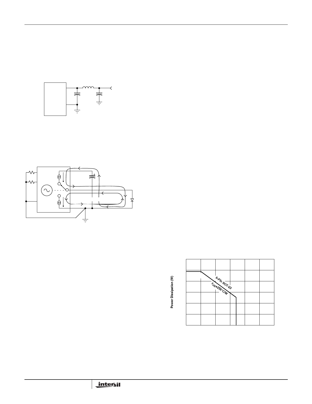
Supply Bypassing and Grounding
The resistance of bypass-capacitors and the inductance of
bonding wires prevent perfect bypass action, and 150mVP-P
noise on the power lines is common. There needs to be a
lossy bead inductance and secondary bypass on the supply
side to control signals from propagating down the wires.
Figure 2 shows the typical connection.
L Series: 70Ω reactance at 300MHz
VS
EL6204
GND
0.1µF
Chip
+5V
0.1µF
Chip
FIGURE 2. RECOMMENDED SUPPLY BYPASSING
Also important is circuit-board layout. At the EL6204's
operating frequencies, even the ground plane is not low-
impedance. High frequency current will create voltage drops
in the ground plane. Figure 3 shows the output current loops.
RFREQ
RAMP
Supply
Bypass
Sourcing Current Loop
GND
Sinking Current Loop
Laser
Diode
FIGURE 3. OUTPUT CURRENT LOOPS
For the pushing current loop, the current flows through the
bypass capacitor, into the EL6204 supply pin, out the IOUT
pin to the laser, and from the laser back to the decoupling
capacitor. This loop should be small.
For the pulling current loop, the current flows into the IOUT
pin, out of the ground pin, to the laser cathode, and from the
laser diode back to the IOUT pin. This loop should also be
small.
Power Dissipation
With the high output drive capability, the EL6204 is possible
to exceed the 125°C “absolute-maximum junction
temperature” under certain conditions. Therefore, it is
important to calculate the maximum junction temperature for
the application to determine if the conditions need to be
modified for the oscillator to remain in the safe operating
area.
The maximum power dissipation allowed in a package is
determined according to:
PDMAX
=
T----J---M-----A----X-----------T----A----M-----A---X--
ΘJA
where
PDMAX = Maximum power dissipation in the package
TJMAX = Maximum junction temperature
TAMAX = Maximum ambient temperature
θJA = Thermal resistance of the package
The supply current of the EL6204 depends on the peak-to-
peak output current and the operating frequency which are
determined by resistors RAMP and RFREQ. The supply
current can be predicted approximately by the following
equation:
ISUP
=
3----1---.--2---5----m-----A------×-----1----k---Ω---
RAMP
+
-3---0----m-----A------×----1----k----Ω---
RFREQ
+
0.6
m
A
The power dissipation can be calculated from the following
equation:
PD = VSUP × ISUP
Here, VSUP is the supply voltage. Figures 4 and 5 provide a
convenient way to see if the device will overheat. The
maximum safe power dissipation can be found graphically,
based on the package type and the ambient temperature. By
using the previous equation, it is a simple matter to see if PD
exceeds the device's power derating curve. To ensure
proper operation, it is important to observe the
recommended derating curve shown in Figures 4 and 5. A
flex circuit may have a higher θJA, and lower power
dissipation would then be required.
Package Power Dissipation vs Ambient Temperature
JEDEC JESD51-3 Low Effective Thermal Conductivity Test Board
0.6
0.5
488mW
0.4
0.3
θJA 6=-2P5i6n°CS/OWT-23
0.2
0.1
0
0
25
50
75 85 100
125
150
Ambient Temperature (°C)
FIGURE 4. PACKAGE POWER DISSIPATION vs
AMBIENT TEMPERATURE
9
Share Link: 