ESD9L3.3ST5G(2009) 데이터 시트보기 (PDF) - ON Semiconductor
부품명
상세내역
제조사
| ESD9L3.3ST5G Datasheet PDF : 0 Pages | |||
ESD9L3.3ST5G
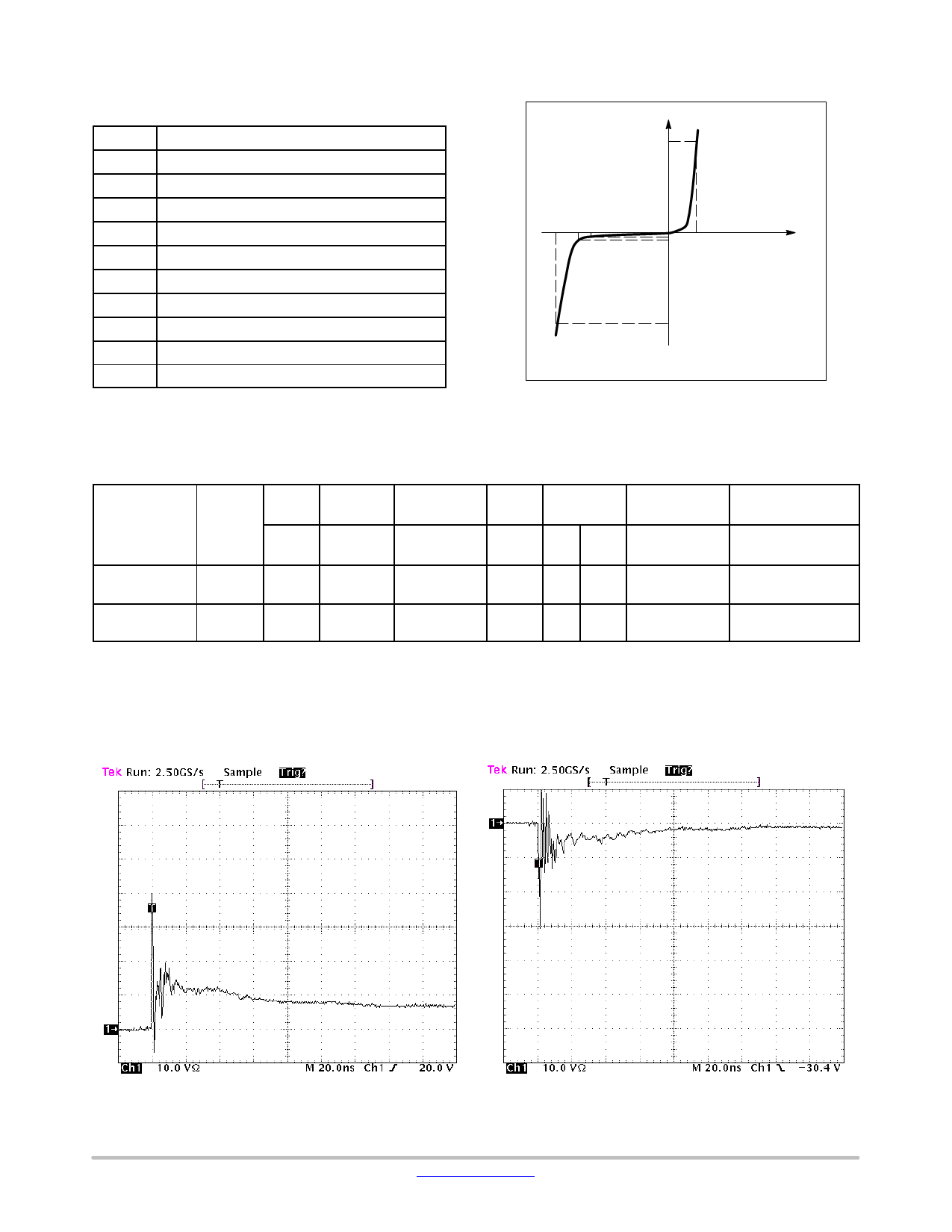
ELECTRICAL CHARACTERISTICS
(TA = 25°C unless otherwise noted)
Symbol
Parameter
IPP
Maximum Reverse Peak Pulse Current
VC
Clamping Voltage @ IPP
VRWM Working Peak Reverse Voltage
IR
Maximum Reverse Leakage Current @ VRWM
VBR Breakdown Voltage @ IT
IT
Test Current
IF
Forward Current
VF
Forward Voltage @ IF
Ppk
Peak Power Dissipation
C
Max. Capacitance @ VR = 0 and f = 1.0 MHz
*See Application Note AND8308/D for detailed explanations of
datasheet parameters.
I
IF
VC VBR VRWM
IIRT VF
V
IPP
Uni−Directional TVS
ELECTRICAL CHARACTERISTICS (TA = 25°C unless otherwise noted, VF = 1.0 V Max. @ IF = 10 mA for all types)
VRWM
IR (mA)
VBR (V) @ IT
VC (V)
(V)
@ VRWM
(Note 2)
IT
C (pF)
@ IPP = 1 A
VC
Device
Device
Marking Max
Max
Per IEC61000−4−2
Min
mA Typ Max
Max
(Note 3)
ESD9L3.3ST5G
6*
3.3
1.0
4.8
1.0 0.5 0.9
9.0
Figures 1 and 2
See Below
*Rotated 180°.
2. VBR is measured with a pulse test current IT at an ambient temperature of 25°C.
3. For test procedure see Figures 3 and 4 and Application Note AND8307/D.
Figure 1. ESD Clamping Voltage Screenshot
Positive 8 kV Contact per IEC61000−4−2
Figure 2. ESD Clamping Voltage Screenshot
Negative 8 kV Contact per IEC61000−4−2
http://onsemi.com
2
Share Link: 