FA5538P 데이터 시트보기 (PDF) - Fuji Electric
부품명
상세내역
제조사
FA5538P Datasheet PDF : 33 Pages
| |||
FA5526/5527/5528/5536/5537/5538
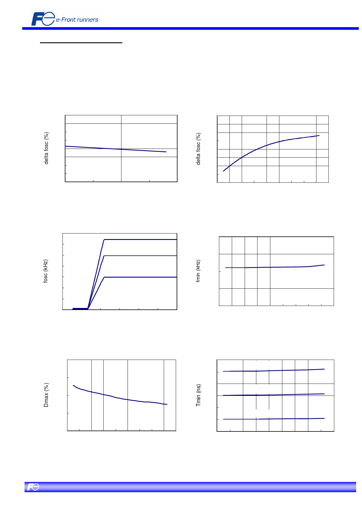
8. Characteristic curves
・Unless otherwise specified, Ta=25℃, Vcc=18V
・In defining a current, “+” represents a sink current and “-” a source current.
・The data stated in this chapter are intended for giving typical IC characteristics and not for guaranteeing performance.
Variation Ratio of Switching Frequency (delta fosc)
vs. VCC pin voltage (Vcc)
2
1.5
1
0.5
0
-0.5
-1
-1.5
-2
10
15
20
25
30
Vcc (V)
Variation Ratio of Switching Frequency (delta fosc)
vs. Junction Temperature (Tj)
2
1.5
1
0.5
0
-0.5
-1
-1.5
-2
-40 -20 0
20 40 60 80 100 120 140
Tj (degree)
140
120
100
80
60
40
20
0
0
Switching Frequency (fosc) vs. FB pin voltage
FA5526 / 36
FA5527 / 37
FA5528 / 38
0.5
1
1.5
2
2.5
3
VFB (V)
Minimum Switching Frequency (fmin) vs. Junction
Temperature (Tj)
2.0
1.5
1.0
0.5
0.0
-40 -20 0 20 40 60 80 100 120 140
Tj(degree)
81.0
Maximum Duty Cycle (Dmax)
vs. Junction Temperature (Tj)
80.5
80.0
79.5
79.0
-40 -20 0
20 40 60 80 100 120 140
Tj(degree)
800
Minimum ON Width (Tmin)
vs. Junction Temperature (Tj)
FA5528 / 38
700
600
FA5527 / 37
500
400
FA5526 / 36
300
200
-40 -20 0
20 40 60 80 100 120 140
Tj(degree)
Fuji Electric Co., Ltd.
AN-087E Rev.1.0
April-2011
10
http://www.fujielectric.co.jp/products/semiconductor/
Share Link: 