FDC05-24S12W 데이터 시트보기 (PDF) - Unspecified
부품명
상세내역
제조사
FDC05-24S12W Datasheet PDF : 2 Pages
| |||
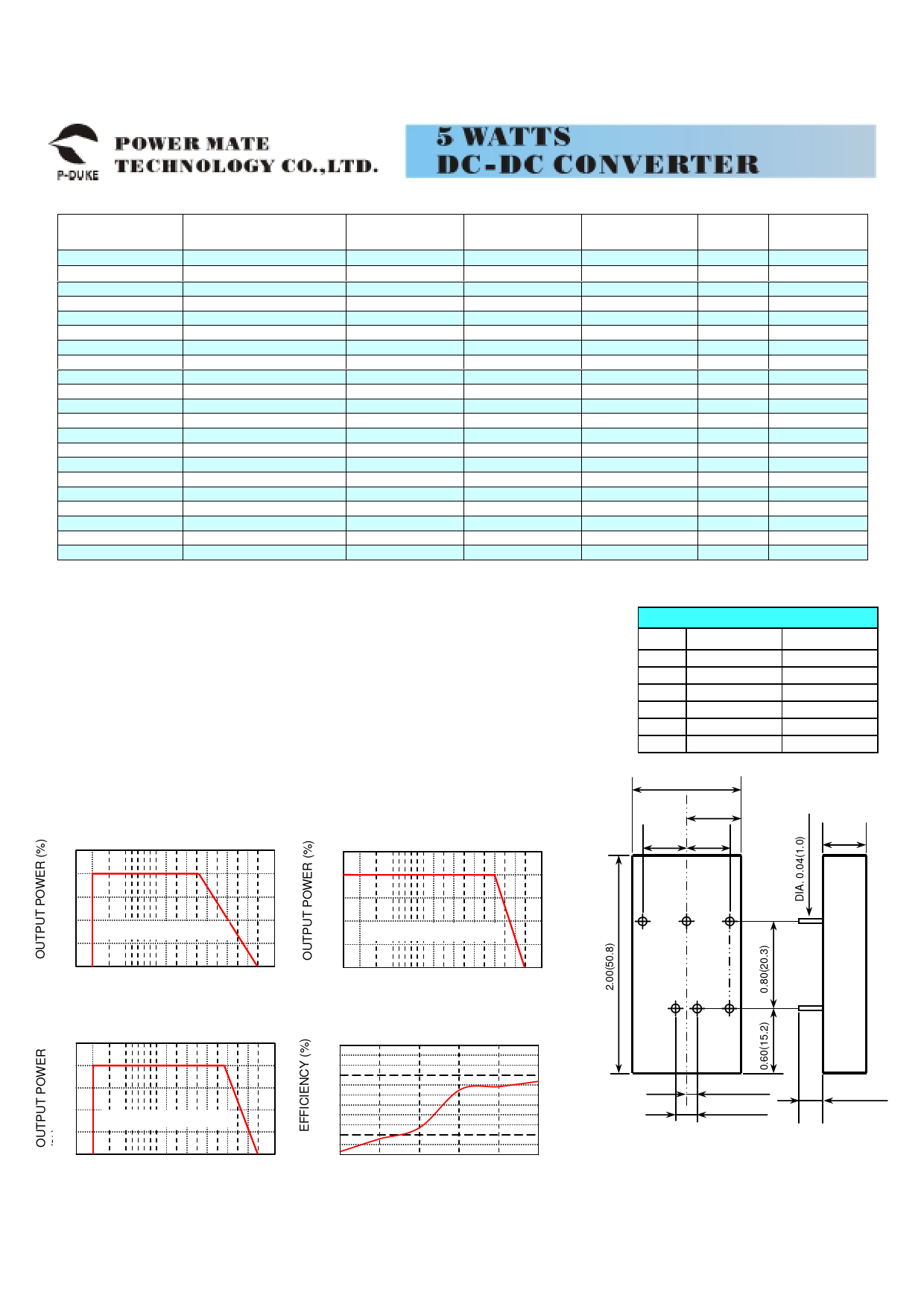
Model
Number
FDC05-12S33
FDC05-12S05
FDC05-12S12
FDC05-12S15
FDC05-12D05
FDC05-12D12
FDC05-12D15
FDC05-24S33 (W)
FDC05-24S05 (W)
FDC05-24S12 (W)
FDC05-24S15 (W)
FDC05-24D05 (W)
FDC05-24D12 (W)
FDC05-24D15 (W)
FDC05-48S33 (W)
FDC05-48S05 (W)
FDC05-48S12 (W)
FDC05-48S15 (W)
FDC05-48D05 (W)
FDC05-48D12 (W)
FDC05-48D15 (W)
Input
Range
9 – 18 VDC
9 – 18 VDC
9 – 18 VDC
9 – 18 VDC
9 – 18 VDC
9 – 18 VDC
9 – 18 VDC
18 – 36 (9 – 36) VDC
18 – 36 (9 – 36) VDC
18 – 36 (9 – 36) VDC
18 – 36 (9 – 36) VDC
18 – 36 (9 – 36) VDC
18 – 36 (9 – 36) VDC
18 – 36 (9 – 36) VDC
36 – 75 (18 – 75) VDC
36 – 75 (18 – 75) VDC
36 – 75 (18 – 75) VDC
36 – 75 (18 – 75) VDC
36 – 75 (18 – 75) VDC
36 – 75 (18 – 75) VDC
36 – 75 (18 – 75) VDC
Output
Voltage
3.3 VDC
5 VDC
12 VDC
15 VDC
± 5 VDC
± 12 VDC
± 15 VDC
3.3 VDC
5 VDC
12 VDC
15 VDC
± 5 VDC
± 12 VDC
± 15 VDC
3.3 VDC
5 VDC
12 VDC
15 VDC
± 5 VDC
± 12 VDC
± 15 VDC
Output
Current
1000mA
1000mA
470mA
400mA
± 500mA
± 230mA
± 190mA
1000mA
1000mA
470mA
400mA
± 500mA
± 230mA
± 190mA
1000mA
1000mA
470mA
400mA
± 500mA
± 230mA
± 190mA
Input
Current (7)
387mA
556mA
610mA
658mA
595mA
597mA
609mA
199 (196mA)
282 (274mA)
305 (301mA)
325 (325mA)
289 (289mA)
295 (295mA)
308 (301mA)
100 (100mA)
145 (149mA)
151 (151mA)
160 (163mA)
149 (149mA)
149 (149mA)
154 (154mA)
Eff (8)
(%)
75
79
81
80
74
81
82
73 (74)
78 (80)
81 (82)
81 (81)
76 (76)
82 (82)
81 (83)
73 (73)
76 (74)
82 (82)
82 (81)
74 (74)
81 (81)
81 (81)
Capacitor
Load max(9)
3700uF
1700uF
290uF
188uF
± 850uF
± 140uF
± 47uF
3700uF
1700uF
290uF
188uF
± 850uF
± 140uF
± 47uF
3700uF
1700uF
290uF
188uF
± 850uF
± 140uF
± 47uF
Note
1. The FDC05 (W) series required a minimum 10% loading on the output to maintain specified
regulation. Operation under no-load condition will not damage these devices, however they may not
meet all listed specification
2. Simulated source impedance of 12uH. 12uH inductor on series with + Vin.
3. The ON/OFF control is option function. There are positive logic and negative logic. The pin voltage is
referenced to negative input
To order positive logic ON-OFF control add the suffix-P (Ex: FDC05-24S05-P)
To order negative logic ON-OFF control add the suffix-N (Ex: FDC05-24S05-N)
4. BELLCORE TR-NWT-000332. Case I: 50% Stress, Temperature at 40ºC.
(Ground fixed and controlled environment)
5. M1 version is more efficient, therefore, it can be operated in a more extensive temperature range than
standard and M2 version.
6. Heat sink is optional and P/N: 7G-0020A.
7. Maximum value at nominal input voltage and full load of standard type.
8. Typical value at nominal input voltage and full load.
9. Test by minimum Vin and constant resistor load.
FDC05-48S05 Derating Curve
FDC05-48S05-M1 Derating Curve
PIN CONNECTION
PIN
SINGLE DUAL OUTPUT
1
+ INPUT
+ INPUT
2
- INPUT
- INPUT
3
+ OUTPUT
+ OUTPUT
4
NO PIN
COMMON
5
- OUTPUT
- OUTPUT
6 CTRL (Option) CTRL (Option)
1.00(25.4)
0.50
(12.7)
0.40 0.40
(10.2) (10.2)
0.40
(10.2)
100
75
50
Nature convection
25
0
-40 -25 -10 0 50 60 70 80 90 100
AMBIENT TEMPERATURE (ºC)
FDC05-48S05 Derating Curve
With HEAT-SINK (Note5)
100
75
50
Nature convection
25
0
-40 -25 -10 0 50 60 70 80 90 100
AMBIENT TEMPERATURE (ºC)
100
75
50
Nature convection
25
0
-40 -25 -10 0 50 60 70 80 90 100
AMBIENT TEMPERATURE (ºC)
FDC05-48S05
Efficiency VS Output load
82
81
80
79
78
77
76
75
70
65
45
0.05 0.2 0.4
0.6 0.8 1.0
OUTPUT LOAD (A)
34 5
Bottom
View
12 6
0.10(2.5)
0.20(5.1)
0.22(5.6)
1. All dimensions in Inches (mm)
2. Pin Pitch tolerance I0.014(0.35)
Share Link: 