FDC6318P 데이터 시트보기 (PDF) - Fairchild Semiconductor
부품명
상세내역
제조사
FDC6318P Datasheet PDF : 5 Pages
| |||
Typical Characteristics
5
ID = -2.5A
4
3
VDS = -4V
-6V
-8V
2
1
0
0
2
4
6
8
Qg, GATE CHARGE (nC)
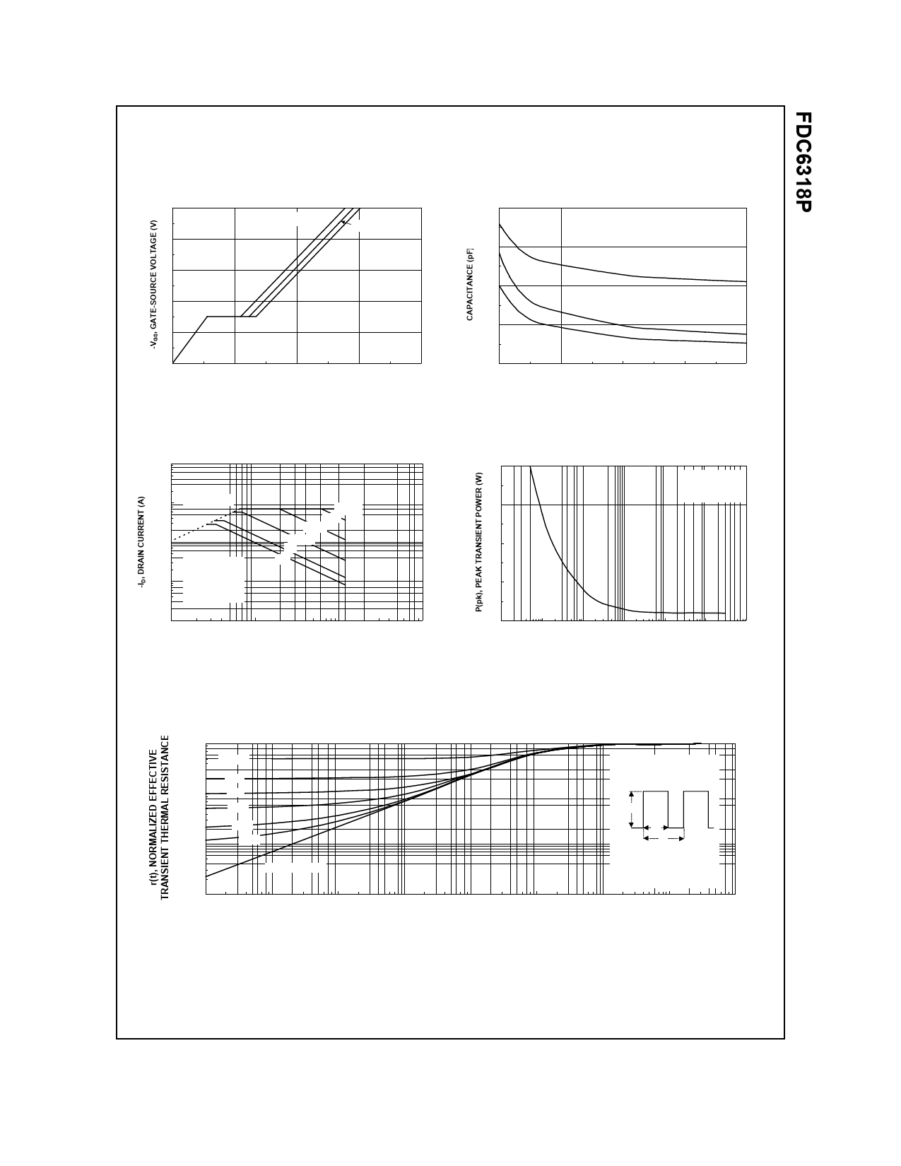
Figure 7. Gate Charge Characteristics.
100
10
RDS(ON) LIMIT
1
VGS = -4.5V
SINGLE PULSE
0.1
RθJA = 130oC/W
TA = 25oC
100µs
1ms
10ms
100ms
1s
DC
0.01
0.1
1
10
100
-VDS, DRAIN-SOURCE VOLTAGE (V)
Figure 9. Maximum Safe Operating Area.
800
600
400
200
0
0
CISS
f = 1 MHz
VGS = 0 V
COSS
CRSS
3
6
9
12
-VDS, DRAIN TO SOURCE VOLTAGE (V)
Figure 8. Capacitance Characteristics.
20
SINGLE PULSE
RθJA = 130°C/W
TA = 25°C
15
10
5
0
0.001
0.01
0.1
1
10
t1, TIME (sec)
100
1000
Figure 10. Single Pulse Maximum
Power Dissipation.
1
0.1
0.01
D = 0.5
0.2
0.1
0.05
0.02
0.01
SINGLE PULSE
RθJA(t) = r(t) * RθJA
RθJA = 130oC/W
P(pk)
t1
t2
TJ - TA = P * RθJA(t)
Duty Cycle, D = t1 / t2
0.001
0.00001
0.0001
0.001
0.01
0.1
1
t1, TIME (sec)
10
100
1000
Figure 11. Transient Thermal Response Curve.
Thermal characterization performed using the conditions described in Note 1b.
Transient thermal response will change depending on the circuit board design.
FDC6318P Rev D (W)
Share Link: 