FDC6327 데이터 시트보기 (PDF) - Fairchild Semiconductor
부품명
상세내역
제조사
FDC6327 Datasheet PDF : 9 Pages
| |||
July 2000
FDC6327C
Dual N & P-Channel 2.5V Specified PowerTrenchTM MOSFET
General Description
These N & P-Channel 2.5V specified MOSFETs are
produced using Fairchild Semiconductor's advanced
PowerTrench process that has been especially tailored
to minimize on-state resistance and yet maintain low gate
charge for superior switching performance.
These devices have been designed to offer exceptional power
dissipation in a very small footprint for applications where
the bigger more expensive SO-8 and TSSOP-8 packages
are impractical.
Applications
• DC/DC converter
• Load switch
• Motor driving
Features
• N-Channel 2.7A, 20V. RDS(on) = 0.08Ω @ VGS = 4.5V
RDS(on) = 0.12Ω @ VGS = 2.5V
• P-Channel -1.6A, -20V.RDS(on) = 0.17Ω @ VGS = -4.5V
RDS(on)= 0.25Ω @ VGS = -2.5V
• Fast switching speed.
• Low gate charge.
• High performance trench technology for extremely
low RDS(ON).
• SuperSOTTM-6 package: small footprint (72% smaller
than SO-8); low profile (1mm thick).
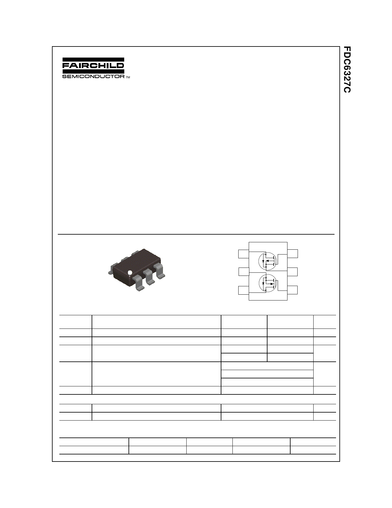
D2
S1
D1
SuperSOT TM -6
G2
S2
G1
4
3
5
2
6
1
Absolute Maximum Ratings TA = 25°C unless otherwise noted
Symbol
Parameter
VDSS
VGSS
ID
Drain-Source Voltage
Gate-Source Voltage
Drain Current - Continuous
- Pulsed
(Note 1a)
PD
Power Dissipation
(Note 1a)
(Note 1b)
(Note 1c)
TJ, Tstg
Operating and Storage Junction Temperature Range
Thermal Characteristics
RθJA
Thermal Resistance, Junction-to-Ambient
RθJC
Thermal Resistance, Junction-to-Case
(Note 1a)
(Note 1)
N-Channel P-Channel
20
-20
±8
±8
2.7
-1.9
8
-8
0.96
0.9
0.7
-55 to +150
130
60
Units
V
V
A
W
°C
°C/W
°C/W
Package Marking and Ordering Information
Device Marking
Device
Reel Size
.327
FDC6327C
7”
Tape Width
8mm
Quantity
3000
1999 Fairchild Semiconductor Corporation
FDC6327C, Rev. E
Share Link: 