FDC6330 데이터 시트보기 (PDF) - Fairchild Semiconductor
부품명
상세내역
제조사
FDC6330 Datasheet PDF : 7 Pages
| |||
Electrical Characteristics TA=25oC unless otherwise noted
Symbol
Parameter
Test Conditions
Min Typ Max Units
OFF Characteristics
IFL
Leakage Current
VIN = 20 V, VON/OFF = 250 µA
1
µA
ON Characteristics (Note 3)
VDROP
Conduction Voltage
VIN = 12 V, VON/OFF = 3.3 V, IL = 2.5 A
0.2
V
VIN = 5 V, VON/OFF = 3.3 V, IL = 1.6 A
0.2
V
R(ON)
Q2 - Static On-Resistance VGS = -12 V, ID = -2.3 A
0.054 0.08
Ω
VGS = -5 V, ID = -1.9 A
0.081 0.125
IL
Load Current
VDROP = 0.2 V, VIN = 12 V, VON/OFF = 3.3 V
2.5
A
VDROP = 0.2 V, VIN = 5 V, VON/OFF = 3.3 V
1.6
Notes:
1. Range of Vin can be up to 30V, but R1 and R2 must be scaled such that VGS of Q2 does not exceed 20V.
2. RθJA is the sum of the junction-to-case and case-to-ambient thermal resistance where the case thermal reference is defined as the solder mounting
surface of the drain pins. RθJC is guaranteed by design while RθJA is determined by the user’s board design.
3. Pulse Test: Pulse Width < 300µs, Duty Cycle < 2.0%.
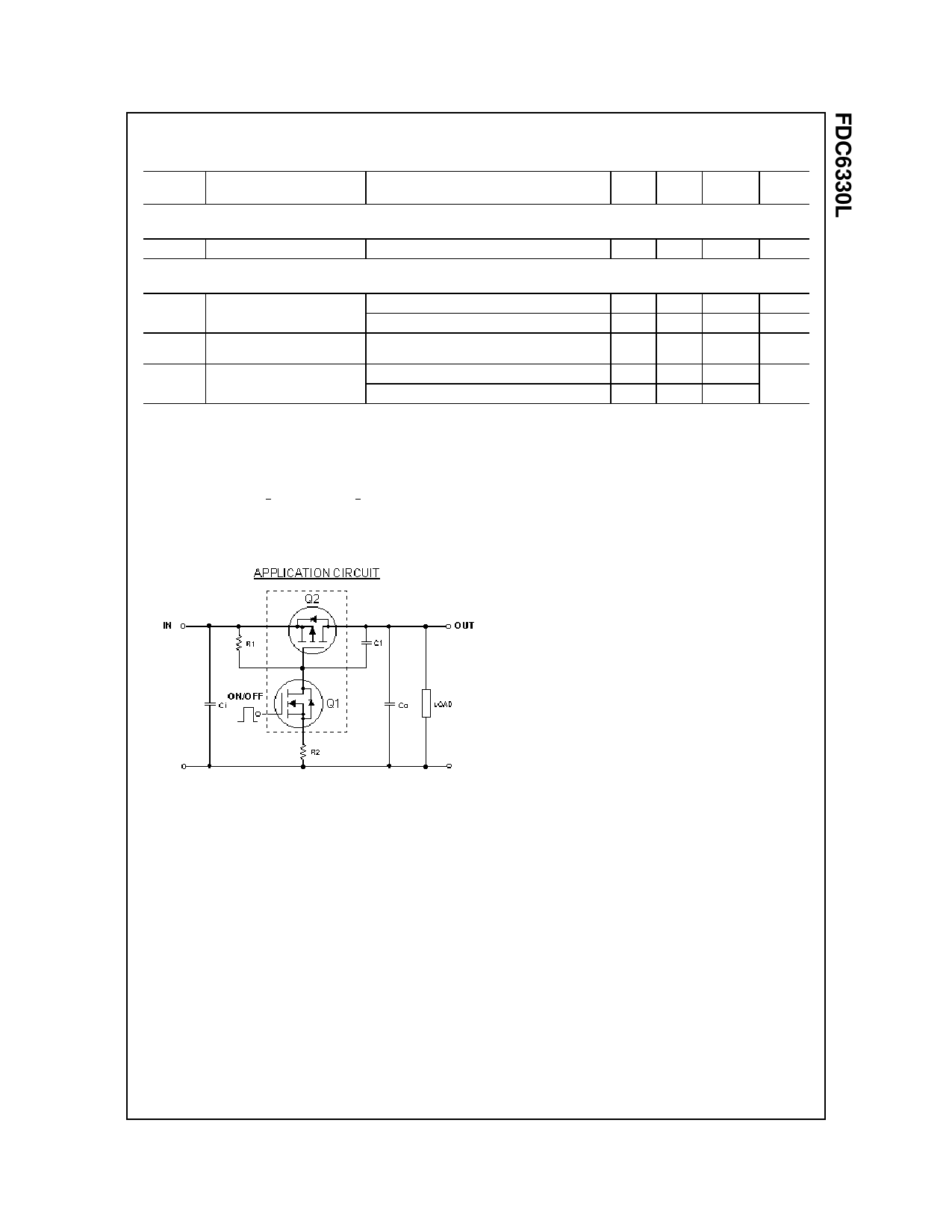
FDC6330L Load Switch Application
External Component Recommendation:
For applications where Co ≤ 1µF.
For slew rate control, select R2 in the range of 1k - 4.7kΩ .
For additional in-rush current control,C1 ≤ 1000pF can be added.
Select R1 so that the R1/R2 ratio ranges from 10 - 100. R1 is required to turn Q2 off.
FDC6330L Rev. C
Share Link: 