FVXO-HC52 데이터 시트보기 (PDF) - Fox Electronics
부품명
상세내역
제조사
FVXO-HC52 Datasheet PDF : 15 Pages
| |||
FVXO-HC52 Series
Electrical Characteristics
Parameters
Frequency Range
Absolute Pull Range Note 1
Temperature Range
Supply Voltage
Input Current (@ 15pF LOAD)
Output Load
Symbol
FO
APR
TO
TSTG
VDD
IDD
HCMOS
Condition
Standard operating
Optional operating
Storage
Standard
0.75 ~ 20 MHz
20+ ~ 50 MHz
50+ ~ 100 MHz
100+ ~ 130 MHz
130+ ~ 160 MHz
160+ ~ 180 MHz
Standard
Maximum Value
(unless otherwise noted)
0.750 to 180.000 MHz
± 50 ppm MIN
-20°C to +70°C
-40°C to +85°C
-55°C to +125°C
2.5V ± 5%
22 mA
25 mA
29 mA
32 mA
35 mA
37 mA
15 pF
Start-Up Time
TS
Output Enable / Disable Time
10 mS
100 nS
Moisture Sensitivity Level
MSL
JEDEC J-STD-20
1
Termination Finish
Au
Note 1 – Inclusive of 25°C tolerance, operating temperature range, input voltage change, load change, aging, shock and vibration.
Frequency Control (VC) Input -- pin # 1
Parameters
Control Voltage Tuning Slope 1
Control Voltage Linearity 2
Control Voltage Tuning Range
Modulation Bandwidth
Symbol
LVC
VC
BW
Condition
0V to VDD
Maximum Value
(unless otherwise noted)
40 ~ 75 ppm/V Typ2
± 10%
0V ~ 2.5V
10 kHz Min
Nominal Control Voltage
VCNOM
@ f0
1.25V
NOTES:
1 Actual slope is affected by frequency and accuracy settings.
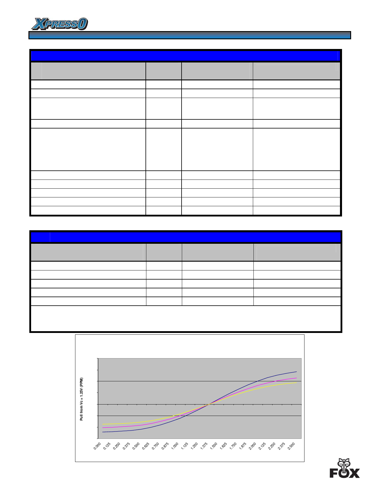
2 For an example of linearity, see the graph below. (The middle line represents the default Fox factory setting)
FVXO Oscillator Pull
@25°C - (range of typical responses)
200.0
150.0
100.0
50.0
0.0
-50.0
-100.0
-150.0
0.000 0.125 0.250 0.375 0.500 0.625 0.750 0.875 1.000 1.125 1.250 1.375 1.500 1.625 1.750 1.875 2.000 2.125 2.250 2.375 2.500
Vc = Voltage applied to Pin #1
Page 3 of 15
© 2008 FOX ELECTRONICS | ISO9001:2000 Certified
Share Link: 