HT819D0 데이터 시트보기 (PDF) - Holtek Semiconductor
부품명
상세내역
제조사
HT819D0 Datasheet PDF : 13 Pages
| |||
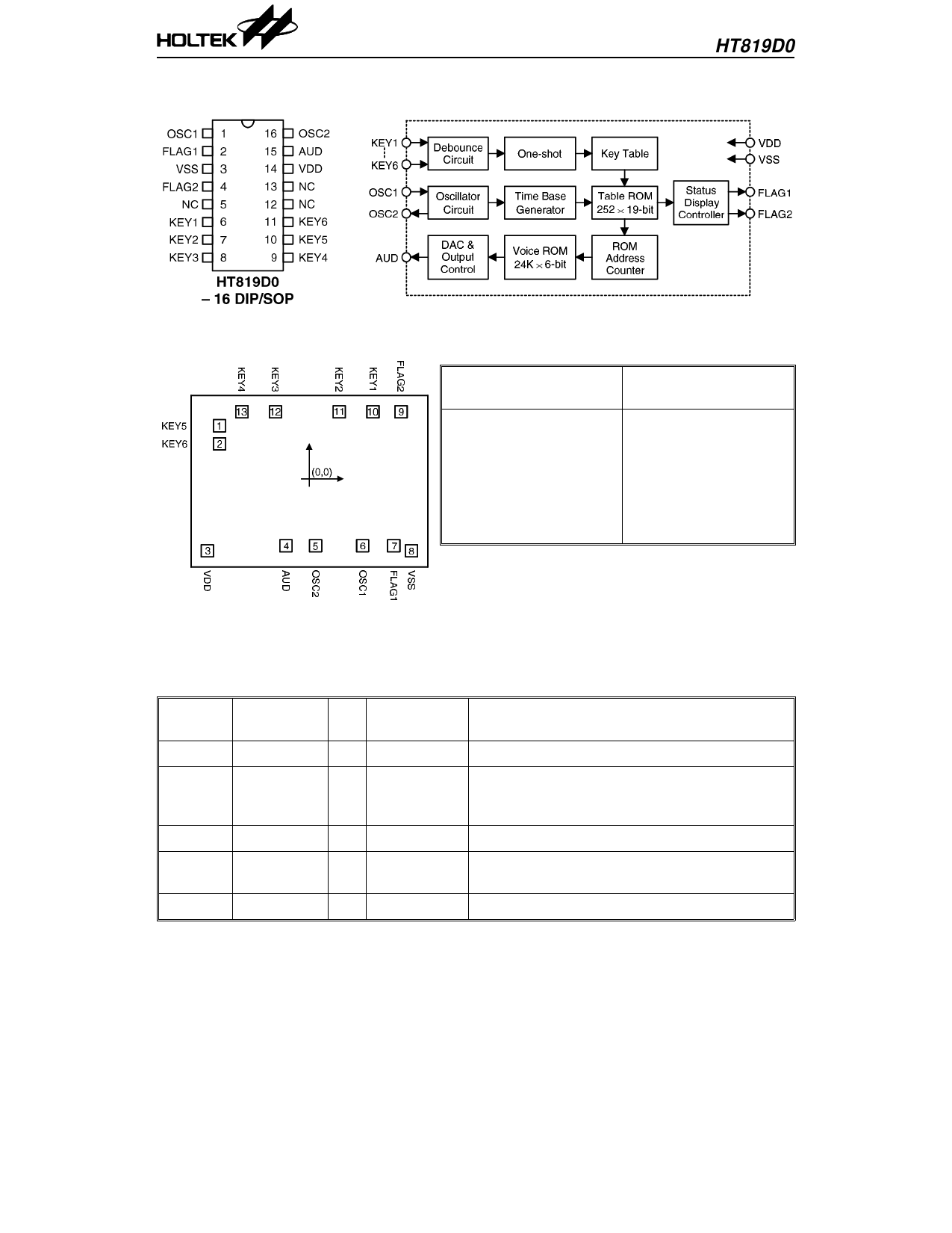
Pin Assignment
Block Diagram
HT819D0
Pad Coordinates
Unit: µm
Pad
No.
X
Y
1 –885.05 522.30
2 –885.05 344.50
3 –1005.05 –710.50
4 –229.95 –660.50
5
62.35 –660.50
6 526.75 –660.50
7 833.85 –660.50
Pad
No.
8
9
10
11
12
13
X
Y
1008.85 –710.50
905.45 660.50
628.05 660.50
296.45 660.50
–333.95 660.50
–665.55 660.50
Chip size: 2290 × 1750 (µm)2
* The IC substrate should be connected to VSS in the PCB layout artwork.
Pin Description
Pin No.
Pin Name
I/O
Internal
Connection
Description
1
OSC1
I
—
Oscillator input pin
2
FLAG1
O
NMOS
Open Drain
3HzB/6HzB flash output, busy output, end-pulse
or voice output indication (by code option). Open
drain, active low output
3
VSS
I
—
Negative power supply (GND)
4
FLAG2
O
NMOS 3Hz/6Hz flash output or busy output (by code
Open Drain option). Open drain, active low output
5, 12, 13 NC
—
—
No connection
2
6th May ’98
Share Link: 