AZ100EL16 데이터 시트보기 (PDF) - AZ Microtek
부품명
상세내역
제조사
AZ100EL16 Datasheet PDF : 6 Pages
| |||
AZ10EL16
AZ100EL16
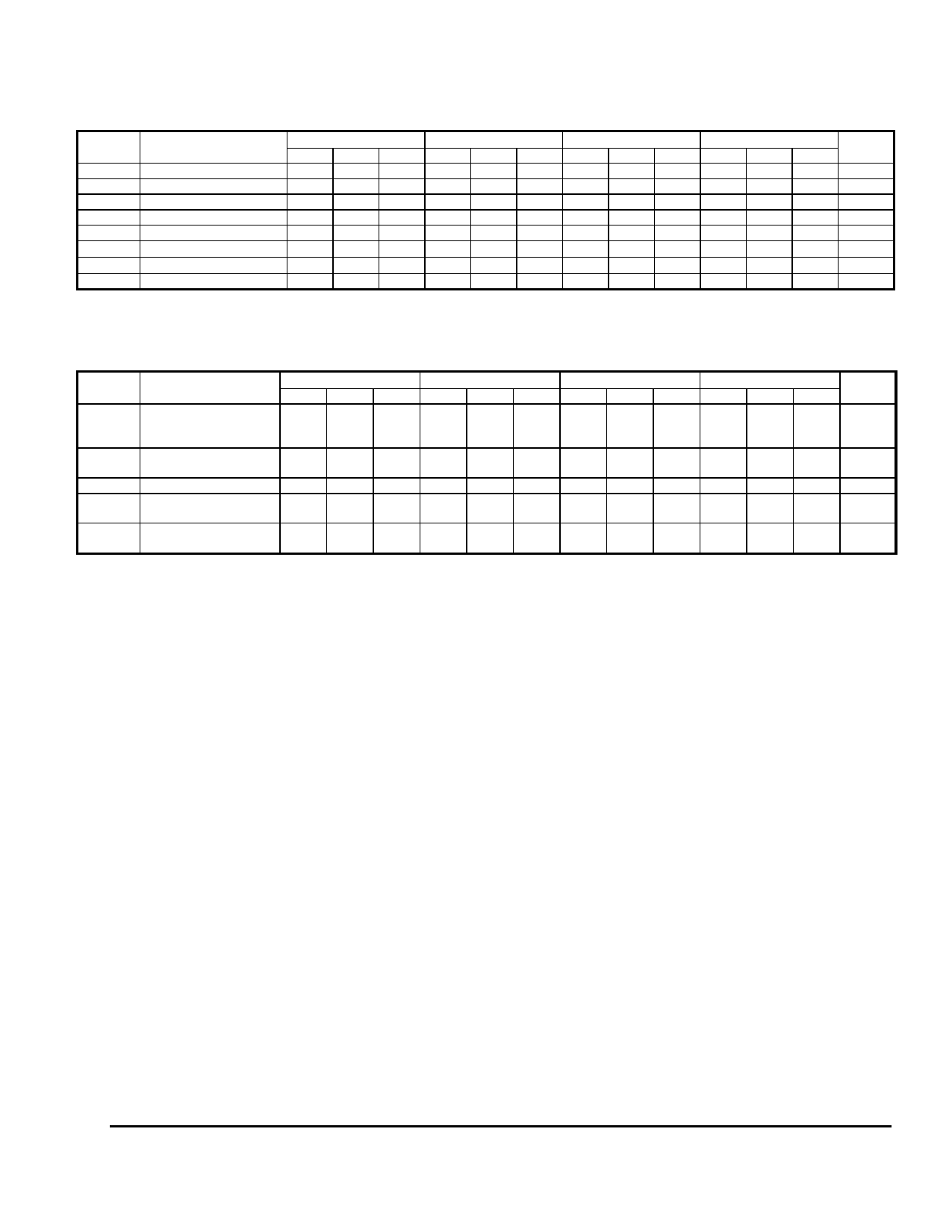
100K PECL DC Characteristics (VEE = GND, VCC = +5.0V)
Symbol
Characteristic
-40°C
0°C
25°C
85°C
Unit
Min Typ Max Min Typ Max Min Typ Max Min Typ Max
VOH
Output HIGH Voltage1,2 3915 3995 4120 3975 4045 4120 3975 4045 4120 3975 4045 4120 mV
VOL
Output LOW Voltage1,2
3170 3305 3445 3190 3295 3380 3190 3295 3380 3190 3295 3380
mV
VIH
Input HIGH Voltage1
3835
4120 3835
4120 3835
4120 3835
4120 mV
VIL
Input LOW Voltage1
3190
3525 3190
3525 3190
3525 3190
3525 mV
VBB
Reference Voltage1
3620
3740 3620
3740 3620
3740 3620
3740 mV
IIH
Input HIGH Current
150
150
150
150
µA
IIL
Input LOW Current
0.5
0.5
0.5
0.5
µA
IEE
Power Supply Current
18
22
18
22
18
22
21
26
mA
1. For supply voltages other that 5.0V, use the ECL table values and ADD supply voltage value.
2. Each output is terminated through a 50Ω resistor to VCC – 2V.
AC Characteristics (VEE =10E(-4.75V to -5.5V), 100E(-4.2V to -5.5V); VCC=GND or VEE =GND; VCC =10E(+4.75V to +5.5V),
100E(+4.2V to +5.5V) )
Symbol
Characteristic
-40°C
0°C
25°C
85°C
Unit
Min Typ Max Min Typ Max Min Typ Max Min Typ Max
tPLH / tPHL
Propagation Delay
to Output
(Diff)
125
250
375
175
250
325
175
250
325
205
280
355
ps
(SE) 75 250 425 125 250 375 125 250 375 155 280 405
tSKEW
Duty Cycle Skew 1
(Diff)
5
5
20
5
20
5
20
ps
VPP (AC) Minimum Input Swing2 150
150
150
150
mV
VCMR
Common Mode Range3
VCC –
2.0
VCC – VCC –
0.4 2.0
VCC – VCC –
0.4 2.0
VCC – VCC –
0.4 2.0
VCC –
0.4
V
tr / tf
Output Rise/Fall Times
Q (20% - 80%)
100
350 100
350 100
350 100
350
ps
1. Duty cycle skew is the difference between a tPLH and tPHL propagation delay through a device.
2. VPP is the minimum peak-to-peak differential input swing for which AC parameters are guaranteed. The device has a DC gain of ≈ 40.
3. The VCMR range is referenced to the most positive side of the differential input signal. Normal operation is obtained if the HIGH level falls within the
specified range and the peak-to-peak voltage lies between VPP (min) and 1V.
October 2001 * REV - 2
www.azmicrotek.com
3
Share Link: 