HI2301 데이터 시트보기 (PDF) - Intersil
부품명
상세내역
제조사
HI2301 Datasheet PDF : 13 Pages
| |||
HI2301
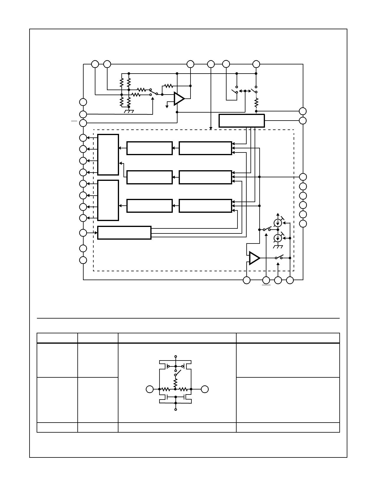
Functional Block Diagram
VIN2 VIN1
27 25
OPO
30
ADV ADV
21 22
AVDD
26
TEST
(DVSS) 19
SEL 4
CE 5
D0 (LSB) 16
D1 15
D2 14
D3 13
D4 12
D5 11
D6 10
D7 (MSB) 9
CLK 18
R
R
3R
-
+
VBI
RTS
REFERENCE
SUPPLY
LOWER
DATA
LATCH
UPPER
DATA
LATCH
LOWER ENCODER
(4-BIT)
LOWER ENCODER
(4-BIT)
UPPER ENCODER
(4-BIT)
LOWER SAMPLING
COMPARATOR (4-BIT)
LOWER SAMPLING
COMPARATOR (4-BIT)
UPPER SAMPLING
COMPARATOR (4-BIT)
ADV
CLOCK GENERATOR
DVDD 17
DVSS 8
A/D CONVERTER
-
+
BLOCK
23 VRT
1 VRB
29 ADIN
2 AVSS
3 AVSS
7 AVSS
28 AVSS
31 AVSS
24
VREF
6 20 32
CLE CLP CCP
Pin Descriptions
PIN NO.
SYMBOL
1
VRB
23
VRT
2, 3, 7, 28, 31
AVSS
EQUIVALENT CIRCUIT
AVDD
RTS
RREF
23
1
AVSS
DESCRIPTION
Reference voltage (bottom) connect to AVSS
for normal use. When another external voltage
is input, connect an external 0.1µF capacitor
and retain a 1.5V differential compared to the
top reference voltage.
Reference voltage (top) by setting VRB to
AVSS, outputs approximately 1.5V. Connect
only a 0.1µF external by-pass capacitor for
normal use. When another external voltage is
input, it must be 2.2V or lower.
Analog GND.
4-2
Share Link: 