HI2301 데이터 시트보기 (PDF) - Intersil
부품명
상세내역
제조사
HI2301 Datasheet PDF : 13 Pages
| |||
HI2301
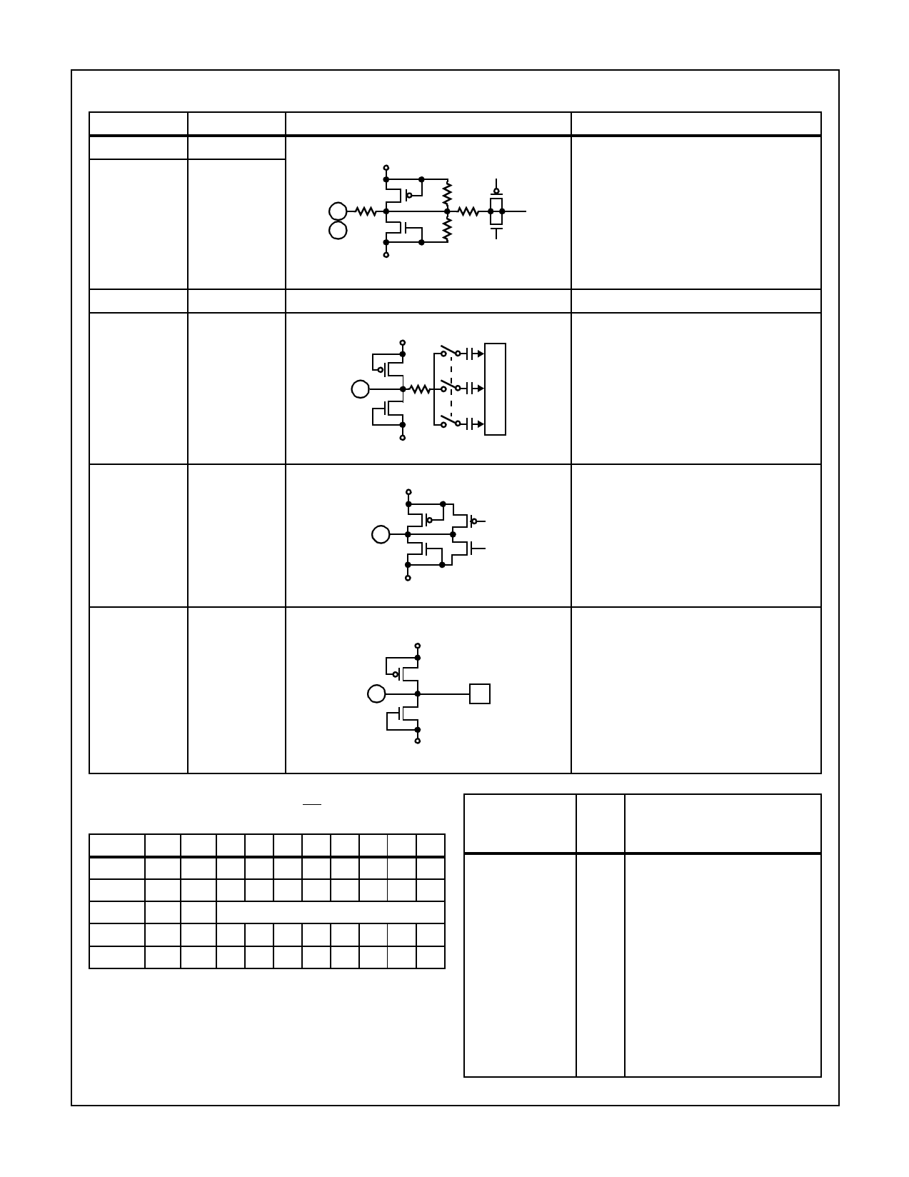
Pin Descriptions (Continued)
PIN NO.
SYMBOL
25
VIN1
27
VIN2
26
AVDD
29
ADIN
EQUIVALENT CIRCUIT
AVDD
200
25
27
AVSS
R11
R
R12
AVDD
DESCRIPTION
Amplifier input pin. Biased internal at 1.9V
(when AVDD = 5V) or at 1.8V (when
AVDD = 4.75V). When standby as well. When
SEL is at Low level, VIN1 is selected for input;
when SEL is at High level, VIN2 is selected for
input.
5V or 4.75V
A/D converter block analog input.
29
30
OPO
32
CCP
AVSS
AVDD
30
AVSS
AVDD
32
Amplifier Output. The phase of this output is
inverted against the phase of VIN1, 2. In
standby mode, it becomes high-impedance
output condition.
Integrates the clamp control voltage. The rela-
tionship between the CCP voltage variation
and the ADIN voltage is positive phase.
AVSS
The following table shows the status of the digital output pins
when the TEST pin is used with the CE and SEL pins.
TEST
L
L
H
H
H
CE SEL D1 D2 D3 D4 D5 D6 D7 D8
L X D1 D2 D3 D4 D5 D6 D7 D8
H X LLLLLLLL
LX
TEST MODE
H L HLHLHLHL
H H LHLHLHLH
Digital Output
The following table shows the correlation between the ADIN
input voltage and the digital output code. Take notice that
the phase of ADIN input signal voltage is inverted against
the phase of the digital output.
ADIN
INPUT SIGNAL
VOLTAGE
VRT
•
•
•
•
•
•
•
•
VRB
DIGITAL OUTPUT CODE
STEP MSB
LSB
0 00000000
•
•
•
•
•
•
127 0 1 1 1 1 1 1 1
128 1 0 0 0 0 0 0 0
•
•
•
•
•
•
255 1 1 1 1 1 1 1 1
4-4
Share Link: 