HT1632C(2015) 데이터 시트보기 (PDF) - Holtek Semiconductor
부품명
상세내역
제조사
HT1632C Datasheet PDF : 25 Pages
| |||
HT1632C
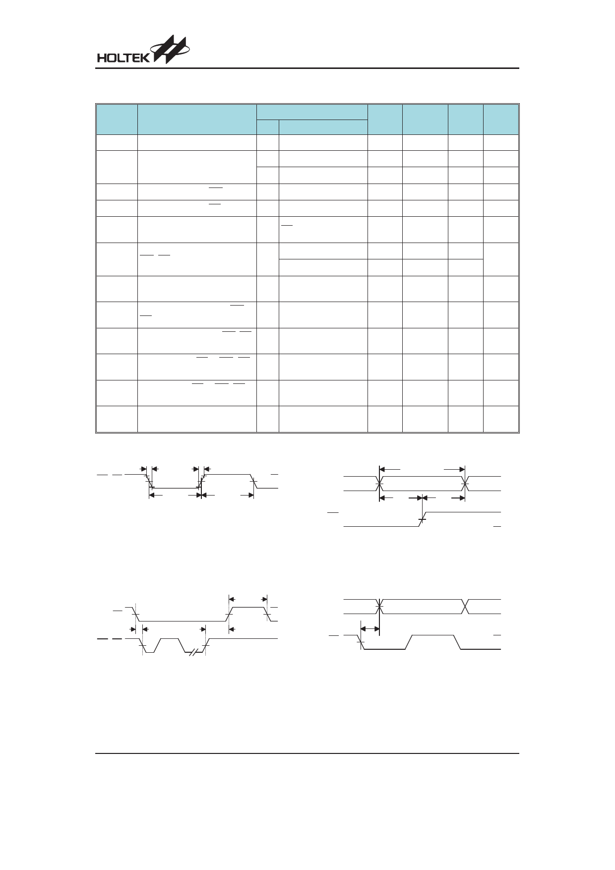
A.C. Characteristics
VDD=2.4V~5.5V, Ta=25°C (Unless otherwise specified)
Symbol
Parameter
fSYS
System Clock
fLED
LED Duty Cycle & Frame
Frequency
fCLK1
Serial Data Clock (WR pin)
fCLK2
Serial Data Clock (RD pin)
tCS
Serial Interface Reset Pulse Width
tCLK
WR, RD Input Pulse Width
tr, tf
Rise/Fall Time Serial Data
Clock Width (Figure 1)
Test Conditions
VDD
Conditions
5V On-chip RC oscillator
1/8 duty
5V
1/16 duty
5V Duty cycle 50%
5V Duty cycle 50%
— CS
Write mode
5V
Read mode
——
Min. Typ. Max.
230
256
282
— fSYS/2624 —
— fSYS/2624 —
—
—
1
—
—
500
250
—
—
0.5
—
—
1.0
—
—
—
50
100
Unit
kHz
Hz
Hz
MHz
kHz
ns
µs
ns
tsu
Setup Time for DATA to WR,
RD Clock Width (Figure 2)
——
50
100
—
ns
th
Hold Time for DATA to WR, RD,
Clock Width (Figure 2)
——
100
200
—
ns
tsu1
Setup Time for CS to WR, RD,
Clock Width (Figure 3)
——
200
300
—
ns
th1
Hold Time for CS to WR, RD,
Clock Width (Figure 3)
——
100
200
—
ns
tod
Data Output Delay Time
(Figure 4)
——
—
100
200
ns
V a lid D a ta
V DD
D ATA
50%
GND
W R ,R D
C lo c k
9
5
0
1
0
%
0
%
%
tf
tC L K
tr
tC L K
V DD
GND
WR
C lo c k
ts u
th
V DD
50%
GND
Figure 1
Figure 2
tC S
CS
50%
tsu 1
th 1
W R ,R D
C lo c k
50%
V DD
GND
D ATA
V DD
GND
RD
50%
to d
V DD
GND
V DD
F ir s t C lo c k
L a s t C lo c k
GND
Figure 3
Figure 4
Rev. 1.60
4
August 19, 2015
Share Link: 