HT19LG(2001) 데이터 시트보기 (PDF) - Supertex Inc
부품명
상세내역
제조사
HT19LG Datasheet PDF : 3 Pages
| |||
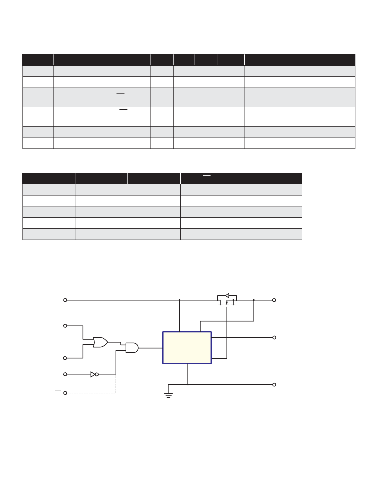
Block Diagram
TPG (1)
(2)
HKS
(5)
LS
(6) for HT18
DP
(6) for HT19
DP
H = ON
L = OFF
Charge Pump
&
Logic Control
HT18/HT19
(8) TP
(7)
CS
(3)
GND
Pin Description
Pin # Symb Description
1 TPG Positive input side of a telephone line, typically Tip side.
2 HKS Hookswitch input. Connect HKS to TPG to turn on the hook switch. Internally pulled low with a high value resistor.
3 GND Device ground. Negative side of a telephone line, typically Ring side.
4 NC No Connect. Open Circuit. No internal connections to the device.
5 LS Line switch input. Input logic high turns on the hook switch. Internally pulled low with a high value resistor.
6 DP For HT18. Dial pulse input. Input logic high turns off the hook switch. Used for pulse dialing. Internally pulled low with a
high value resistor.
6 DP For HT19. Dial pulse input. Input logic low turns off the hook switch. Used for pulse dialing. Internally pulled high with a
high value resistor.
7 CS Current sense input. An external resistor connected between CS and TP sets the current limit.
8 TP Positive output side of a telephone line. Zener protection to prevent this output from rising above 18V is required.
Typical Application Circuit
Tip
Transient
Protection
Ring
TPG
TP
RSEN
HT18
HKS
or
HT19
GND
CS
LS
DP/DP
15V Telecom
Circuit
©2001 Supertex Inc. All rights reserved. Unauthorized use or reproduction prohibited.
3
12/13/010
1235 Bordeaux Drive, Sunnyvale, CA 94089
TEL: (408) 744-0100 • FAX: (408) 222-4895
www.supertex.com
Share Link: 