HT46R49 데이터 시트보기 (PDF) - Holtek Semiconductor
부품명
상세내역
제조사
HT46R49 Datasheet PDF : 77 Pages
| |||
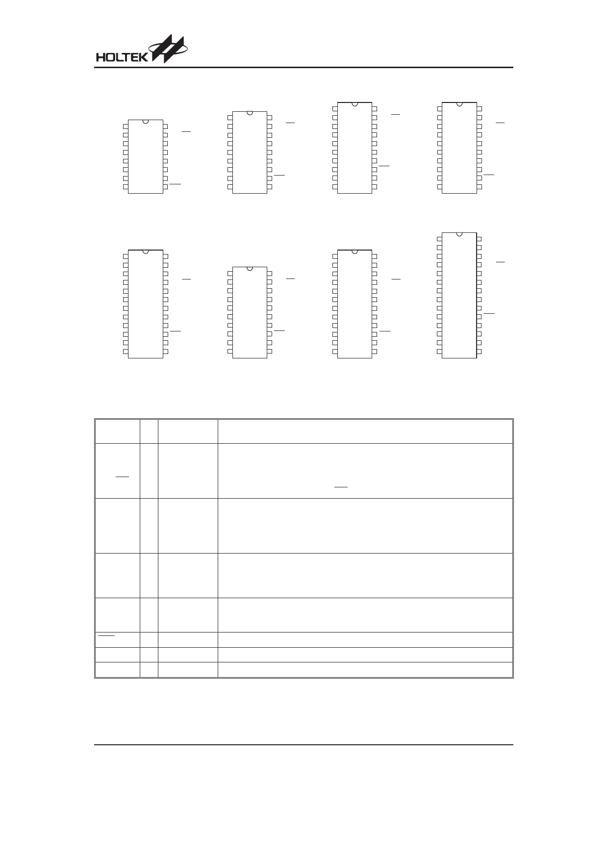
HT46R46/C46/R47/C47/R48A/C48A/R49
Pin Assignment
P A 3 /P F D 1
PA2 2
PA1 3
PA0 4
P B 1 /A N 1 5
P B 0 /A N 0 6
VSS 7
P D 0 /P W M
8
1 6 P A 4 /T M R
1 5 P A 5 /IN T
14 P A 6
13 P A 7
12 O S C 2
11 O S C 1
10 V D D
9 RES
H T 4 6 R 4 6 /H T 4 6 C 4 6
H T 4 6 R 4 7 /H T 4 6 C 4 7
1 6 N S O P -A
P A 3 /P F D 1
PA2 2
PA1 3
PA0 4
P B 3 /A N 3 5
P B 2 /A N 2 6
P B 1 /A N 1 7
P B 0 /A N 0 8
VSS 9
1 8 P A 4 /T M R
1 7 P A 5 /IN T
16 P A 6
15 P A 7
14 O S C 2
13 O S C 1
12 V D D
11 R E S
1 0 P D 0 /P W M
H T 4 6 R 4 6 /H T 4 6 C 4 6
H T 4 6 R 4 7 /H T 4 6 C 4 7
1 8 D IP -A /S O P -A
P A 3 /P F D 1
PA2 2
PA1 3
PA0 4
P B 3 /A N 3 5
NC 6
P B 2 /A N 2 7
P B 1 /A N 1 8
P B 0 /A N 0 9
V S S 10
2 0 P A 4 /T M R
1 9 P A 5 /IN T
18 P A 6
17 P A 7
16 O S C 2
15 O S C 1
14 V D D
13 R E S
1 2 P D 0 /P W M
11 N C
H T 4 6 R 4 6 /H T 4 6 C 4 6
H T 4 6 R 4 7 /H T 4 6 C 4 7
2 0 S S O P -A
PB4 1
P A 3 /P F D 2
PA2 3
PA1 4
PA0 5
P B 3 /A N 3 6
P B 2 /A N 2 7
P B 1 /A N 1 8
P B 0 /A N 0 9
V S S 10
20 P B 5
1 9 P A 4 /T M R
1 8 P A 5 /IN T
17 P A 6
16 P A 7
15 O S C 2
14 O S C 1
13 V D D
12 R E S
1 1 P D 0 /P W M
H T 4 6 R 4 8 A /H T 4 6 C 4 8 A
2 0 D IP -A /S O P -A
PB5 1
PB4 2
P A 3 /P F D 3
PA2 4
PA1 5
PA0 6
P B 3 /A N 3 7
P B 2 /A N 2 8
P B 1 /A N 1 9
P B 0 /A N 0 1 0
V S S 11
P C 0 12
24 P B 6
23 P B 7
2 2 P A 4 /T M R
2 1 P A 5 /IN T
20 P A 6
19 P A 7
18 O S C 2
17 O S C 1
16 V D D
15 R E S
1 4 P D 0 /P W M
13 P C 1
H T 4 6 R 4 8 A /H T 4 6 C 4 8 A
2 4 S K D IP -A /S O P -A /S S O P -A
P A 3 /P F D 1
20
PA2 2
19
PA1 3
18
PA0 4
17
P B 3 /A N 3 5
16
P B 2 /A N 2 6
15
P B 1 /A N 1 7
14
P B 0 /A N 0 8
13
VSS 9
12
P C 0 10
11
H T46R 49
2 0 D IP -A /S O P -A
P A 4 /T M R
P A 5 /IN T
PA6
PA7
O SC2
O SC1
VDD
RES
P D 1 /P W M 1
P D 0 /P W M 0
PB5 1
PB4 2
P A 3 /P F D 3
PA2 4
PA1 5
PA0 6
P B 3 /A N 3 7
P B 2 /A N 2 8
P B 1 /A N 1 9
P B 0 /A N 0 1 0
V S S 11
P C 0 12
24 P B 6
23 P B 7
2 2 P A 4 /T M R
2 1 P A 5 /IN T
20 P A 6
19 P A 7
18 O S C 2
17 O S C 1
16 V D D
15 R E S
1 4 P D 1 /P W M 1
1 3 P D 0 /P W M 0
H T46R 49
2 4 S K D IP -B /S O P -B
PB5 1
PB4 2
P A 3 /P F D 3
PA2 4
PA1 5
PA0 6
P B 3 /A N 3 7
P B 2 /A N 2 8
P B 1 /A N 1 9
P B 0 /A N 0 1 0
V S S 11
P C 0 12
P C 1 13
P C 2 14
28 P B 6
27 P B 7
2 6 P A 4 /T M R
2 5 P A 5 /IN T
24 P A 6
23 P A 7
22 O S C 2
21 O S C 1
20 V D D
19 R E S
1 8 P D 1 /P W M 1
1 7 P D 0 /P W M 0
16 P C 4
15 P C 3
H T46R 49
2 8 S K D IP -A /S O P -A
Pin Description
HT46R46, HT46R47
Pin Name
I/O
Configuration
Option
Description
PA0~PA2
PA3/PFD
PA4/TMR I/O
PA5/INT
PA6~PA7
Pull-high
Wake-up
PA3 or PFD
Bidirectional 8-bit input/output port. Each individual pin on this port can be config-
ured as a wake-up input by a configuration option. Software instructions determine
if the pin is a CMOS output or Schmitt Trigger input. Configuration options deter-
mine which pins on the port have pull-high resistors. Pins PA3, PA4 and PA5 are
pin-shared with PFD, TMR and INT, respectively.
PB0/AN0
PB1/AN1
PB2/AN2
I/O
PB3/AN3
Pull-high
Bidirectional 4-bit input/output port. Software instructions determine if the pin is a
CMOS output or Schmitt Trigger input. Configuration options determine which pins
on the port have pull-high resistors. PB is pin-shared with the A/D input pins. The
A/D inputs are selected via software instructions. Once selected as an A/D input,
the I/O function and pull-high resistor options are disabled automatically.
PD0/PWM I/O
Pull-high
PD0 or PWM
Bidirectional 1-bit input/output port. Software instructions determine if the pin is a
CMOS output or Schmitt Trigger input.
A configuration option determines if this pin has a pull-high resistor. The PWM out-
put is pin-shared with pin PD0 selected via a configuration option.
OSC1
OSC2
I
O
Crystal
or RC
OSC1, OSC2 are connected to an external RC network or external crystal, deter-
mined by configuration option, for the internal system clock. If the RC system clock op-
tion is selected, pin OSC2 can be used to measure the system clock at 1/4 frequency.
RES
I
¾
Schmitt Trigger reset input. Active low.
VDD
¾
¾
Positive power supply
VSS
¾
¾
Negative power supply, ground
Note:
1. Each pin on PA can be programmed through a configuration option to have a wake-up function.
2. Individual pins can be selected to have a pull-high resistor.
3. Pins PB2/AN2~PB3/AN3 exist but are not bonded out on the 16-pin package.
4. unbonded pins should be setup as outputs or as inputs with pull-high resistors to conserve power.
Rev. 1.30
3
June 5, 2008
Share Link: 