HT49CV3 데이터 시트보기 (PDF) - Holtek Semiconductor
부품명
상세내역
제조사
HT49CV3 Datasheet PDF : 44 Pages
| |||
HT49RV3/HT49CV3
Stack Register - STACK
The stack register is a special part of the memory used
to save the contents of the Program Counter. The stack
is organized into 6 levels and is neither part of the data
nor part of the program, and is neither readable nor
writeable. Its activated level is indexed by a stack
pointer (SP) and is neither readable nor writeable. At the
start of a subroutine call or an interrupt acknowledg-
ment, the contents of the Program Counter is pushed
onto the stack. At the end of the subroutine or interrupt
routine, signaled by a return instruction (RET or RETI),
the contents of the Program Counter is restored to its
previous value from the stack. After a chip reset, the SP
will point to the top of the stack.
If the stack is full and a non-masked interrupt takes
place, the interrupt request flag is recorded but the ac-
knowledgment is still inhibited. Once the SP is decre-
mented (by RET or RETI), the interrupt is serviced. This
feature prevents stack overflow, allowing the program-
mer to use the structure easily. Likewise, if the stack is
full, and a ²CALL² is subsequently executed, a stack
overflow occurs and the first entry is lost (only the most
recent 6 return addresses are stored).
Data Memory - RAM
The data memory (RAM) has a capacity of 130´8 bits,
and is divided into two functional groups, namely; spe-
cial function registers (34´8 bit) and general purpose
data memory (RAM bank contains 96´8 bits) most of
which are readable/writeable, but some are read only.
The special function registers are overlapped in any
banks.
The special function registers consist of an Indirect ad-
dressing register 0 (00H), a Memory pointer register 0
(MP0;01H), an Indirect addressing register 1 (02H), a
Memory pointer register 1 (MP1;03H), a Bank pointer
(BP;04H), an Accumulator (ACC;05H), a Program coun-
ter lower-order byte register (PCL;06H), a Table pointer
(TBLP;07H), a Table higher-order byte register
(TBLH;08H), a Real time clock control register
(RTCC;09H), a Status register (STATUS;0AH), an Inter-
rupt control register 0 (INTC0;0BH), a Timer/Event
Counter 0 (TMR0H:0CH; TMR0L:0DH), a Timer/Event
Counter 0 control register (TMR0C;0EH), a Timer/Event
Counter 1 (TMR1H:0FH;TMR1L:10H), a Timer/Event
Counter 1 control register (TMR1C; 11H), Interrupt con-
trol register 1 (INTC1;1EH), Serial Bus control register
(SBCR;1FH), Serial Bus data register (SBDR; 20H), Re-
mote timer control register (RMTC;21H), Remote con-
trol capture register 0 (RMT0;22H), Remote control
capture register 1 (RMT1;23H), Multi-function interrupt
Status register (MFIS;29H), VFD control register
(VFDC; 28H), I/O registers (PA;12H, PB;14H, PC;16H,
PD;18H) and I/O control registers (PAC;13H, PBC;15H,
PCC;17H, PDC;19H).
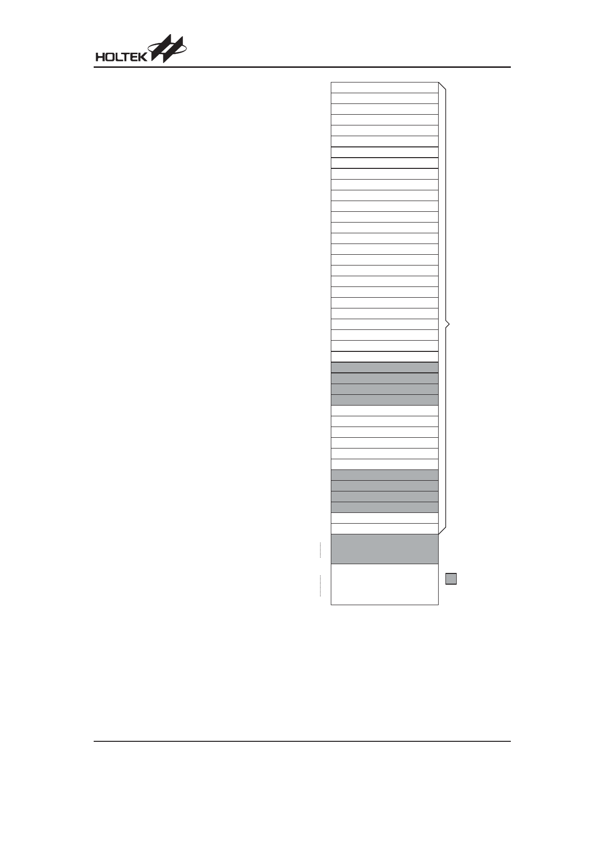
00H
In d ir e c t A d d r e s s in g R e g is te r 0
01H
M P0
02H
In d ir e c t A d d r e s s in g R e g is te r 1
03H
M P1
04H
BP
05H
ACC
06H
PCL
07H
TB LP
08H
TB LH
09H
R TC C
0A H
STATU S
0B H
IN T C 0
0C H
TM R 0H
0D H
TM R 0L
0E H
TM R 0C
0FH
TM R 1H
10H
TM R 1L
11H
TM R 1C
12H
PA
13H
PAC
14H
PB
15H
PBC
16H
PC
17H
PCC
18H
PD
19H
PDC
1A H
PW M 0
1B H
PW M 1
1C H
PW M 2
1D H
PW M 3
1E H
IN T C 1
1FH
SBCR
20H
SBDR
21H
R M TC
22H
R M T0
23H
R M T1
24H
25H
ADR
26H
ADCR
27H
ACSR
28H
VFD C
29H
M F IS
30H
S p e c ia l P u r p o s e
D a ta M e m o ry
3FH
40H
G e n e ra l P u rp o s e
D a ta M e m o ry
:U nused
(9 6 B y te s )
R e a d a s "0 0 "
9FH
RAM Mapping
The remaining space before 40H is reserved for future
expansion usage and reading these locations will return
the result ²00H². The space before 40H overlaps in
each bank. The general-purpose data memory, ad-
dressed from 40H to 9FH, is used for data and control
information under instruction commands.
Rev. 1.30
8
March 20, 2007
Share Link: 