HT66FU60 데이터 시트보기 (PDF) - Holtek Semiconductor
부품명
상세내역
제조사
HT66FU60 Datasheet PDF : 246 Pages
| |||
HT66F20/HT66F30/HT66F40/HT66F50/HT66F60
HT66FU30/HT66FU40/HT66FU50/HT66FU60
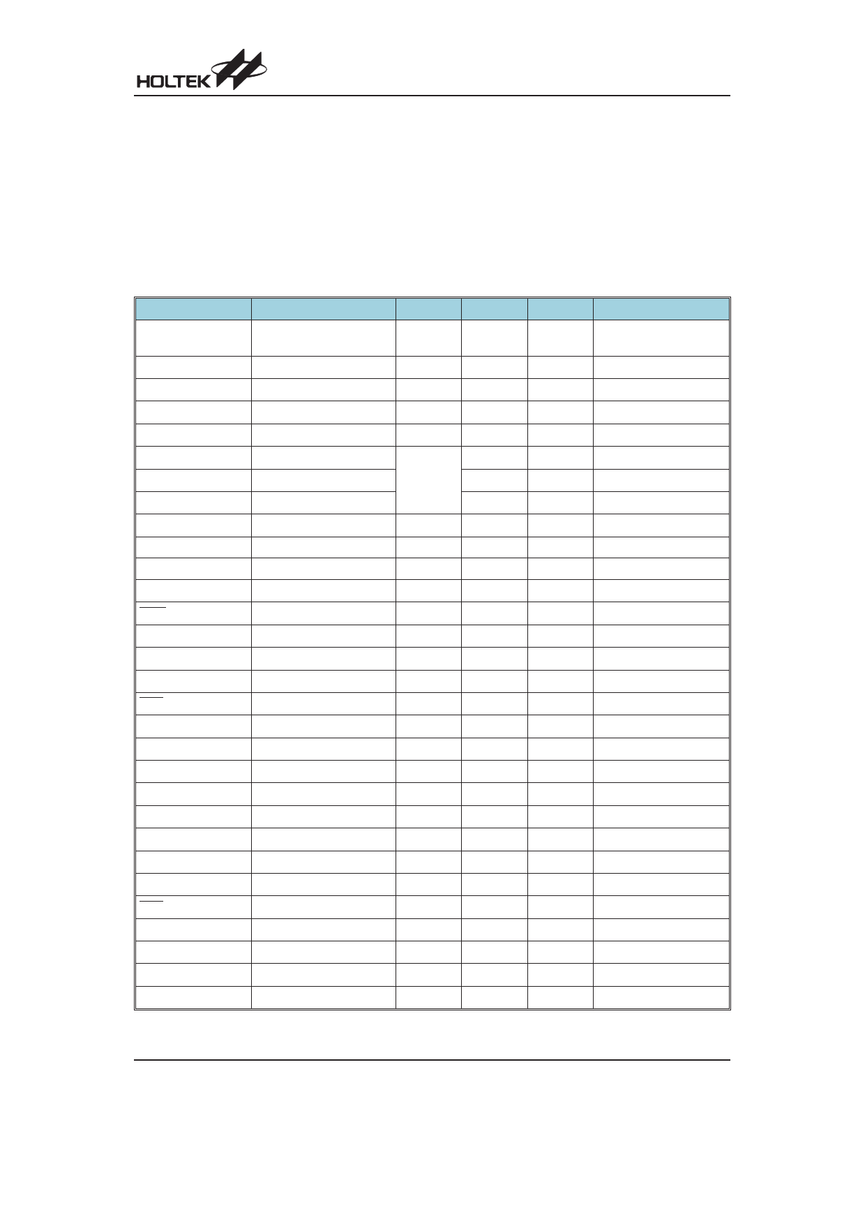
Pin Description
With the exception of the power pins, all pins on these devices can be referenced by their Port name, e.g. PA.0, PA.1
etc, which refer to the digital I/O function of the pins. However these Port pins are also shared with other function such
as the Analog to Digital Converter, Serial Port pins etc. The function of each pin is listed in the following table, however
the details behind how each pin is configured is contained in other sections of the datasheet.
The following tables only include the pins which are directly related to the MCU. The pin descriptions of the additional
peripheral functions are located at the end of the datasheet along with the relevant peripheral function functional de-
scription.
HT66F20
Pin Name
PA0~PA7
PB0~PB5
PC0~PC3
AN0~AN7
VREF
C0-, C1-
C0+, C1+
C0X, C1X
TCK0, TCK1
TP0_0
TP1_0, TP1_1
INT0, INT1
PINT
PCK
SDI
SDO
SCS
SCK
SCL
SDA
SCOM0~SCOM3
OSC1
OSC2
XT1
XT2
RES
VDD
AVDD
VSS
AVSS
Function
Port A
Port B
Port C
ADC input
ADC reference input
Comparator 0, 1 input
Comparator 0, 1 input
Comparator 0, 1 output
TM0, TM1 input
TM0 I/O
TM1 I/O
Ext. Interrupt 0, 1
Peripheral Interrupt
Peripheral Clock output
SPI Data input
SPI Data output
SPI Slave Select
SPI Serial Clock
I2C Clock
I2C Data
SCOM0~SCOM3
HXT/ERC pin
HXT pin
LXT pin
LXT pin
Reset input
Power supply *
ADC power supply *
Ground **
ADC ground **
OP
PAWU
PAPU
PBPU
PCPU
ACERL
ADCR1
CP0C
CP1C
¾
TMPC0
TMPC0
¾
¾
¾
¾
¾
¾
¾
¾
¾
SCOMC
CO
CO
CO
CO
CO
¾
¾
¾
¾
I/T
ST
ST
ST
AN
AN
AN
AN
¾
ST
ST
ST
ST
ST
¾
ST
¾
ST
ST
ST
ST
¾
HXT
¾
LXT
¾
ST
PWR
PWR
PWR
PWR
O/T
Pin-Shared Mapping
CMOS ¾
CMOS
CMOS
¾
¾
¾
¾
CMOS
¾
CMOS
CMOS
¾
¾
CMOS
¾
CMOS
CMOS
CMOS
NMOS
NMOS
SCOM
¾
HXT
¾
LXT
¾
¾
¾
¾
¾
¾
¾
PA0~PA7
PB5
PA3, PC3
PA2, PC2
PA0, PA5
PA2, PA4
PA0
PA1, PC0
PA3, PA4
PC3
PC2
PA6
PA5
PB5
PA7
PA7
PA6
PC0, PC1, PC2, PC3
PB1
PB2
PB3
PB4
PB0
¾
¾
¾
¾
Rev. 1.10
7
February 1, 2010
Share Link: 