HT82V36 데이터 시트보기 (PDF) - Holtek Semiconductor
부품명
상세내역
제조사
HT82V36 Datasheet PDF : 10 Pages
| |||
HT82V36
Internal Register Descriptions
Register
Name
Address
A2 A1 A0
Configuration 0
0
0
Reserved
Reserved
PGA
Reserved
Reserved
Offset
Reserved
0
0
1
0
1
0
0
1
1
1
0
0
1
0
1
1
1
0
1
1
1
Data Bits
D8 D7 D6 D5 D4 D3 D2 D1 D0
0
0
1
1
CDS on
Clamp
Voltage
Enable
Power
Down
Output
Delay
1byte
out
X
0
0 MSB
LSB
MSB
LSB
Internal Register Map
D8
D7
D6
D5
D4
D3
D2
D1
D0
CDS operation Clamp bias Power-down
Set to 0 Set to 0 Set to 1 Set to 1 1=CDS mode* 1=2.5V* 1=On
Output delay
1 byte out
(High-byte only)
1=On
1=On
0=SHA mode 0=2V
0=Off (Normal)* 0=Off*
0=Off*
Configuration Register Settings
Note: * Power-on default value
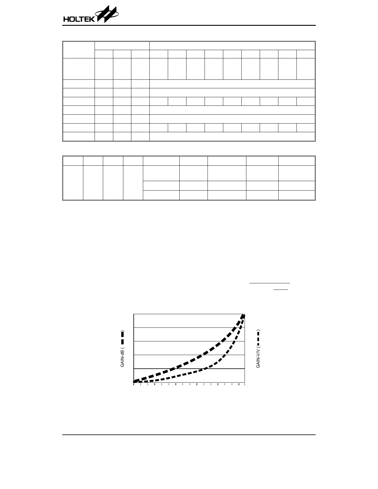
PGA Gain Register
Bits D7 and D6 in the register must be set low, and bits D5 through D0 control the gain range in 64 increments. See fig-
ure for a graph of the PGA gain versus PGA register code. The coding for the PGA register is straight binary, with an all
zero words corresponding to the minimum gain setting (1x) and an all one word corresponding to the maximum gain
setting (5.85x).
The PGA has a gain range from 1x (0dB) to 5.85x (15.3dB), adjustable in 64 steps. The Figure shows the PGA gain as a
function of the PGA register code. Although the gain curve is approximately linear in dB, the gain in V/V varies in non-
linear
proportion
with
the
register
code,
according
to
the
following
the
equation:
Gain=
1+
5.85
4.85 ´´ ( 63
-
G)
63
Where G is the decimal value of the gain register contents, and varies from 0 to 63.
15
5 .8 5
12
5 .0
9
4 .0
6
3 .0
3
2 .0
0
1 .0
0 4 8 12 16 20 24 28 32 36 40 44 48 52 56 60 63
P G A r e g is te r v a lu e - - D e c im a l
PGA Gain Transfer Function
Rev. 1.30
5
June 29, 2004
Share Link: 