HT82V36 데이터 시트보기 (PDF) - Holtek Semiconductor
부품명
상세내역
제조사
HT82V36 Datasheet PDF : 10 Pages
| |||
HT82V36
D8
D7
D6
D5
D4
D3
D2
D1
Set to 0 Set to 0 Set to 0 MSB
0
0
0
0
0
0
0
0
0
0
0
0
0
0
0
0
.
.
.
0
0
0
1
1
1
1
1
0
0
0
1
1
1
1
1
Note: * Power-on default value
PGA Gain Register Settings
D0
Gain
(V/V)
Gain (dB)
LSB
0*
1.0
0.0
1
1.013 0.12
.
.
.
.
.
.
0
5.43
14.7
1
5.85
15.3
Offset Register
Bits D8 through D0 control the offset range from -200mV to 200mV in 512 increments.
The coding for the offset registers is sign magnitude, with D8 as the sign bit. The Table shows the offset range as a
function of the bits D8 through D0.
D8
D7
D6
D5
D4
D3
D2
D1
D0
Offset
(mV)
MSB
LSB
0
0
0
0
0
0
0
0
0*
0
0
0
0
0
0
0
0
0
1
0.78
.
.
.
.
.
.
0
1
1
1
1
1
1
1
1
200
1
0
0
0
0
0
0
0
0
0
1
0
0
0
0
0
0
0
1
-0.78
.
.
.
.
.
.
1
1
1
1
1
1
1
1
1
-200
Note: * Power-on default value
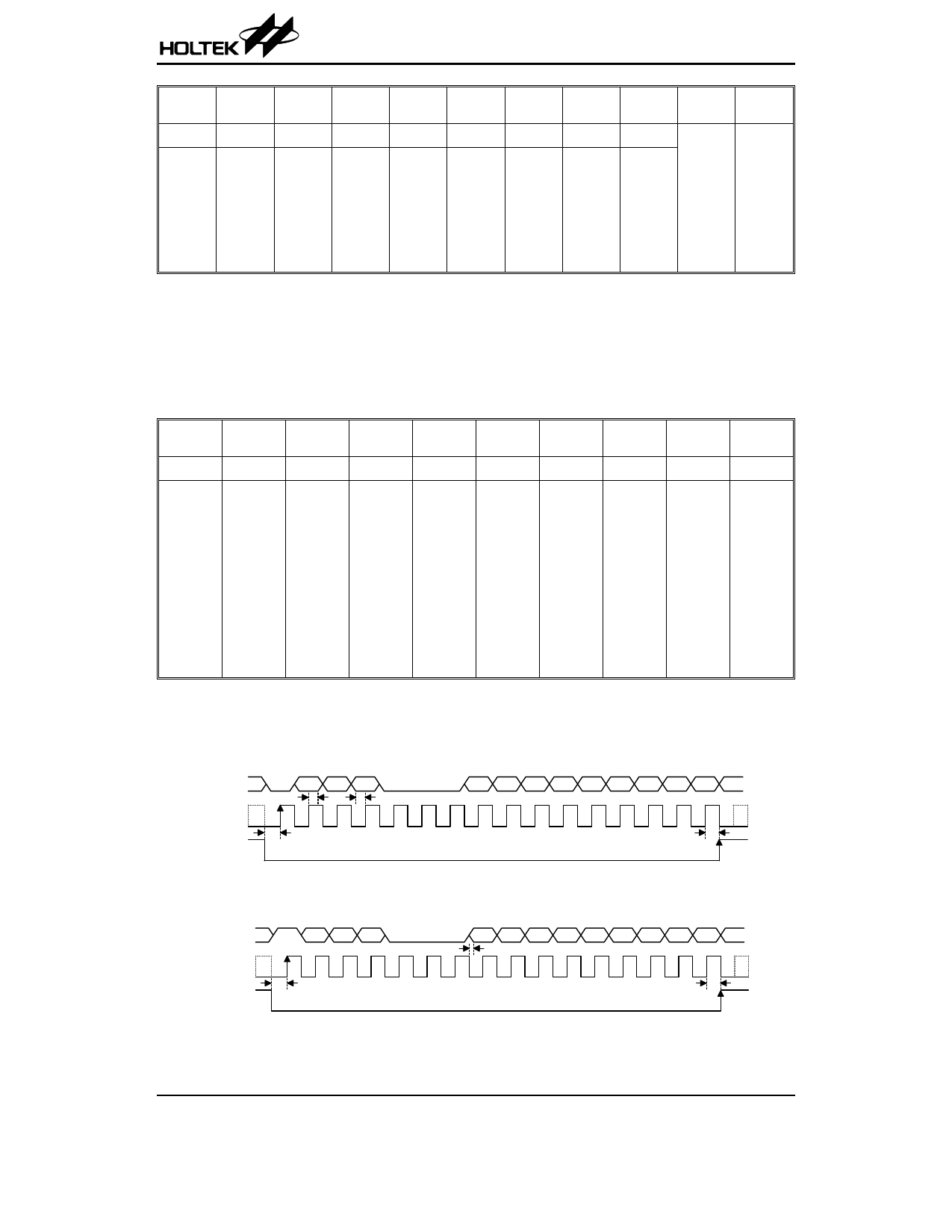
Timing Diagrams
SD ATA
S C LK
S LO A D
R /W b A 2 A 1 A 0
tD H
tD S
tL S
D8 D7 D6 D5 D4 D3 D2 D1 D0
tL H
Serial Write Operation Timing
SD ATA
S C LK
S LO A D
R /W b A 2 A 1 A 0
tL S
D8 D7 D6 D5 D4 D3 D2 D1 D0
tR D V
tL H
Serial Read Operation Timing
Rev. 1.30
6
June 29, 2004
Share Link: 