HT9320 데이터 시트보기 (PDF) - Holtek Semiconductor
부품명
상세내역
제조사
HT9320 Datasheet PDF : 29 Pages
| |||
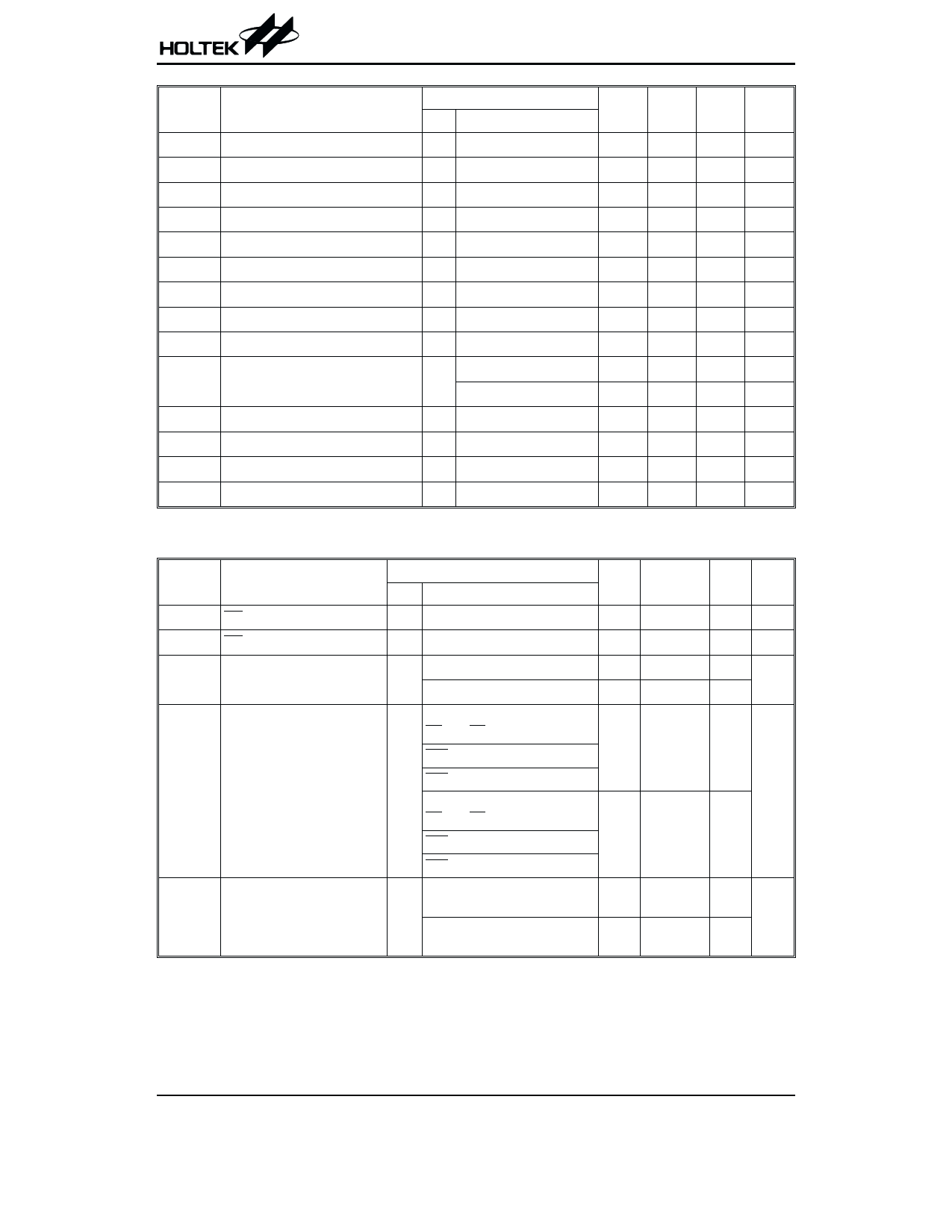
HT9320 Series
Symbol
Parameter
Test Conditions
VDD
Conditions
RHST HST Pull-low Resistance
2.5V VHST=2.5V
IOH1
Keypad Pin Source Current
2.5V VOH=0V
IOL1
Keypad Pin Sink Current
2.5V VOL=2.5V
IOH2
HFO Pin Source Current
2.5V VOH=2V
IOL2
HFO Pin Sink Current
2.5V VOL=0.5V
IOH3
HDO Pin Source Current
2.5V VOH=2V
IOL3
HDO Pin Sink Current
2.5V VOL=0.5V
IOH4
KT Pin Source Current
2.5V VOH=2V
IOL4
KT Pin Sink Current
2.5V VOL=0.5V
TFP
Pause Time After Flash
Control key
¾
Digit key
TRP
Pause Time for One-key Redialing ¾ One-key redialing
TDB
Key-in Debounce Time
¾
¾
TBRK Break Time for One-key Redialing ¾ One-key redialing
fOSC
System Frequency
¾ Crystal=3.5795MHz
Min. Typ. Max. Unit
¾
200
¾
kW
-4
¾ -40 mA
200 400
¾
mA
-1
¾
¾
mA
1
¾
¾
mA
-1
¾
¾
mA
1
¾
¾
mA
-1
¾
¾
mA
1
¾
¾
mA
¾
0.2
¾
s
¾
1
¾
s
¾
1
¾
s
¾
20
¾
ms
¾
1.2
¾
s
3.5759 3.5795 3.5831 MHz
Pulse Mode Electrical Characteristics
fOSC=3.5795MHz, Ta=25°C
Symbol
Parameter
IPOH
PO Output Source Current
Test Conditions
VDD
Conditions
2.5V VOH=2V
Min.
-0.2
Typ.
¾
Max. Unit
¾ mA
IPOL
PO Output Sink Current
2.5V VOL=0.5V
0.2
0.6
¾ mA
PR
Pulse Rate
MODE pin is connected to VDD ¾
10
¾
¾
pps
MODE pin is opened
¾
20
¾
A resistor is linked between
R2 and C1 (HT9320B/C/K/L)
M/B=VSS (HT9320A)
¾
33:66
¾
M/B
Make/Break Ratio
M/B=VDD (HT9320H)
¾
No resistor is linked between
R2 and C1 (HT9320B/C/K/L)
M/B=Floating (HT9320A)
¾
40:60
%
¾
M/B=VSS (HT9320H)
TPDP Pre-digit-pause Time
M/B ratio=40:60
¾
M/B ratio=33:66
¾
40 (10pps)
20 (20pps)
¾
ms
¾
33 (10pps)
17 (20pps)
¾
Rev. 1.10
7
October 1, 2002
Share Link: 