HT82K94E 데이터 시트보기 (PDF) - Holtek Semiconductor
부품명
상세내역
제조사
HT82K94E Datasheet PDF : 43 Pages
| |||
HT82K94E/HT82K94A
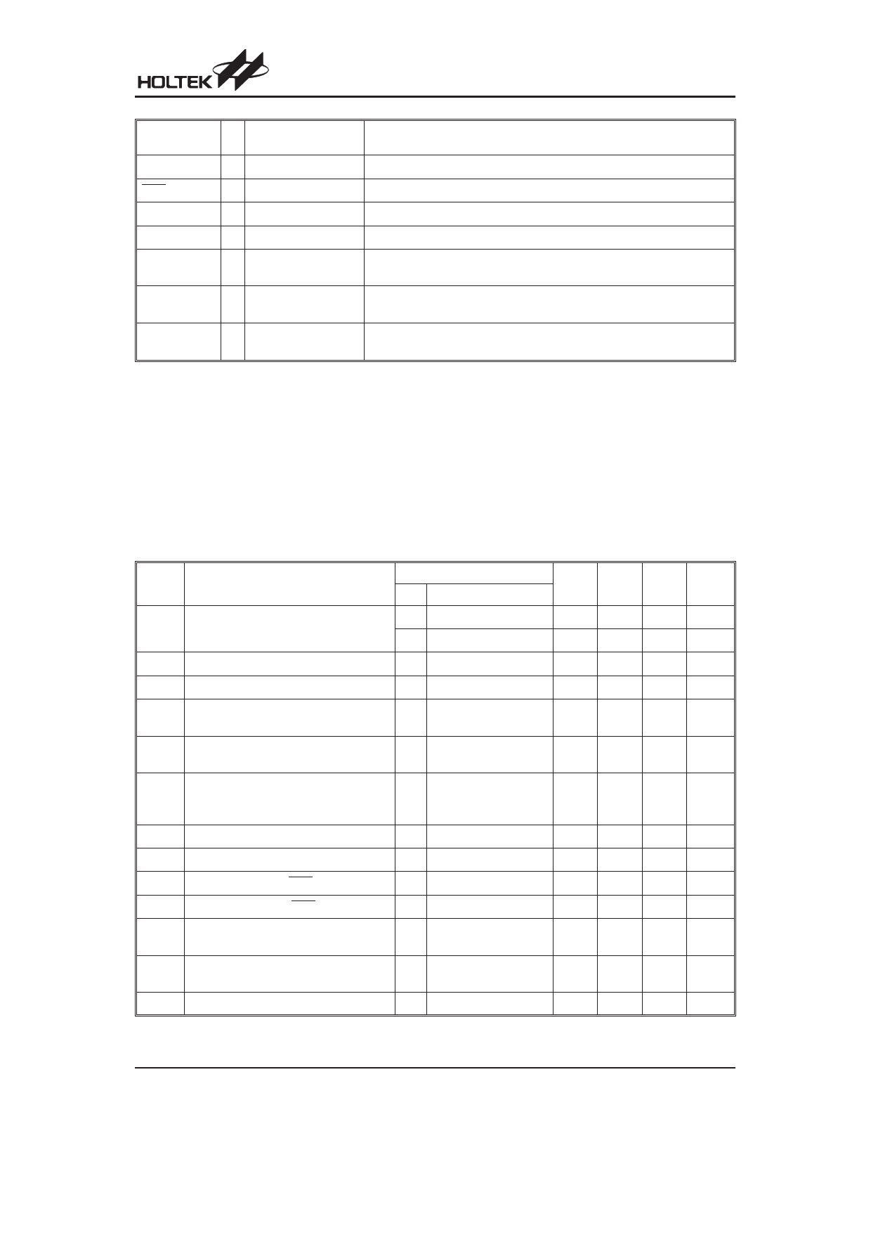
Pin Name I/O
VSS
¾
RES
I
VDD
¾
V33O
O
USBD+/CLK I/O
USBD-/DATA I/O
OSC1
I
OSC2
O
ROM Code
Option
¾
¾
¾
¾
¾
¾
¾
Description
Negative power supply, ground
Schmitt trigger reset input. Active low
Positive power supply
3.3V regulator output
USBD+ or PS2 CLK I/O line
USB or PS2 function is controlled by software control register
USBD- or PS2 DATA I/O line
USB or PS2 function is controlled by software control register
OSC1, OSC2 are connected to a 6MHz or 12MHz Crystal/resonator
(determined by software instructions) for the internal system clock.
Absolute Maximum Ratings
Supply Voltage ...........................VSS-0.3V to VSS+6.0V
Input Voltage..............................VSS-0.3V to VDD+0.3V
Storage Temperature ............................-50°C to 125°C
Operating Temperature...............................0°C to 70°C
Note: These are stress ratings only. Stresses exceeding the range specified under ²Absolute Maximum Ratings² may
cause substantial damage to the device. Functional operation of this device at other conditions beyond those listed
in the specification is not implied and prolonged exposure to extreme conditions may affect device reliability.
D.C. Characteristics
Symbol
Parameter
VDD Operating Voltage
IDD1
IDD2
ISTB1
Operating Current (6MHz Crystal)
Operating Current (12MHz Crystal)
Standby Current (WDT Enabled)
ISTB2 Standby Current (WDT Disabled)
ISTB3 Standby Current (WDT Enabled)
VIL1 Input Low Voltage for I/O Ports
VIH1 Input High Voltage for I/O Ports
VIL2 Input Low Voltage (RES)
VIH2 Input High Voltage (RES)
IOL1
I/O Port Sink Current for PA1~PA7,
PB, PC, PD
IOL2
I/O Port Sink Current for PA1~PA7,
PB, PC, PD
IOL3 I/O Port Sink Current for PA0
Ta=25°C
Test Conditions
VDD
Conditions
Min. Typ. Max. Unit
¾ fSYS=6MHz
2.2
¾
5.5
V
¾ fSYS=12MHz
2.2
¾
5.5
V
5V No load, fSYS=6MHz
¾
6.5
12
mA
5V No load, fSYS=12MHz ¾
7.5
16
mA
5V
No load, system HALT,
USB suspend
¾
¾ 250 mA
5V
No load, system HALT,
USB suspend
¾
¾ 230 mA
No load, system HALT,
5V input/output mode,
¾
¾
15
mA
set SUSPEND2 [1EH]
5V TTL level
0
¾
0.8
V
5V TTL level
2
¾
5
V
5V CMOS level
5V CMOS level
0
¾ 0.4VDD V
0.9VDD ¾
VDD
V
5V VOL=3.4V
10
15
20
mA
5V VOL=0.4V
5V VOL=0.4V
2
4
8
mA
7
10
13
mA
Rev. 1.50
4
October 11, 2007
Share Link: 