HV2301(2011) 데이터 시트보기 (PDF) - Supertex Inc
부품명
상세내역
제조사
HV2301
(Rev.:2011)
(Rev.:2011)
Supertex Inc

HV2301 Datasheet PDF : 9 Pages
| |||
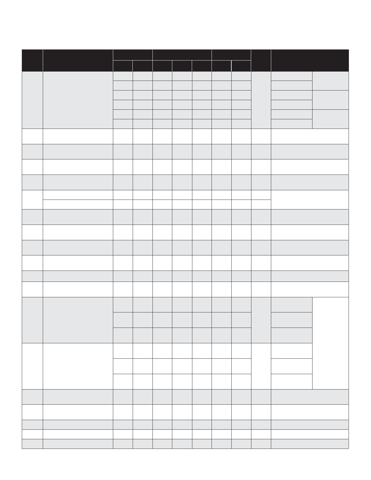
HV2301
DC Electrical Characteristics
(Over operating conditions unless otherwise specified )
Sym Parameter
0OC
Min Max
+25OC
Min Typ Max
+70OC
Min Max
Units Conditions
- 30 - 26 38 - 48
- 25 - 22 27 - 32
ISIG = 5.0mA
ISIG = 200mA
VPP = +40V
VNN = -160V
-
RONS Small signal switch on-resistance
-
25
18
-
-
22 27
18 24
-
-
30
27
Ω
ISIG = 5.0mA
ISIG = 200mA
VPP = +100V
VNN = -100V
- 23 - 20 25 - 30
- 22 - 16 25 - 27
ISIG = 5.0mA
ISIG = 200mA
VPP = +160V
VNN = -40V
ΔRONS
Small signal switch on-resistance
matching
-
20
-
5.0 20
-
20
%
ISIG = 5.0mA, VPP = +100V,
VNN = - 100V
RONL Large signal switch on-resistance -
-
- 15 -
-
-
Ω VSIG = VPP -10V, ISIG = 1.0A
RINT Value of output bleed resistance
-
- 20 35 50 -
-
KΩ
Output switch to RGND
IRINT = 0.5mA
ISOL Switch off leakage per switch
-
5.0
-
1.0 10
-
15
μA VSIG = VPP -10V, VNN +10V
DC offset switch off
VOS DC offset switch on
- 300 - 100 300 - 300 mV
No load
- 500 - 100 500 - 500 mV
IPPQ Quiescent VPP supply current
INNQ Quiescent VNN supply current
IPPQ Quiescent VPP supply current
INNQ Quiescent VNN supply current
ISW Switch output peak current
fSW Output switching frequency
IPP Average VPP supply current
INN Average VNN supply curent
IDD Average VDD supply current
IDDQ Quiescent VDD supply current
ISOR Data out source current
ISINK Data out sink current
CIN Logic input capacitance
-
-
- 10 50 -
-
-
-
- -10 -50 -
-
-
-
- 10 50 -
-
-
-
- -10 -50 -
-
- 3.0 - 3.0 2.0 - 2.0
-
-
-
- 50 -
-
- 4.0 -
- 5.0 - 5.5
- 3.5 -
- 3.5 - 3.5
- 3.5 -
- 3.5 - 4.0
- 4.5 -
- 5.0 - 5.5
- 3.5 -
- 3.5 - 3.5
- 3.5 -
- 3.5 - 4.0
- 4.0 -
- 4.0 - 4.0
- 10 -
- 10 - 10
0.45 - 0.45 0.70 - 0.40 -
0.45 - 0.45 0.70 - 0.40 -
- 10 -
- 10 - 10
μA All switches off
μA All switches off
μA All switches on, ISW = 5.0mA
μA All switches on, ISW = 5.0mA
A VSIG duty cycly < 0.1%
kHz Duty cycle = 50%
VPP = +40V
VNN = -160V
mA
VPP = +100V
VNN = -100V
VPP = +160V
VNN = -40V
VPP = +40V
VNN = -160V
mA
VPP = +100V
VNN = -100V
VPP = +160V
VNN = -40V
All output
switches are
turning on and
off at 50kHz
with no load
All output
switches are
turning on and
off at 50kHz
with no load
mA fCLK = 5.0MHz, VDD = 5.0V
μA All logic inputs are static
mA VOUT = VDD -0.7V
mA VOUT = 0.7V
pF ---
Supertex inc. ● 1235 Bordeaux Drive, Sunnyvale, CA 94089 ● Tel: 408-222-8888 ● www.supertex.com
3
Share Link: