HV301 데이터 시트보기 (PDF) - Supertex Inc
부품명
상세내역
제조사
HV301 Datasheet PDF : 20 Pages
| |||
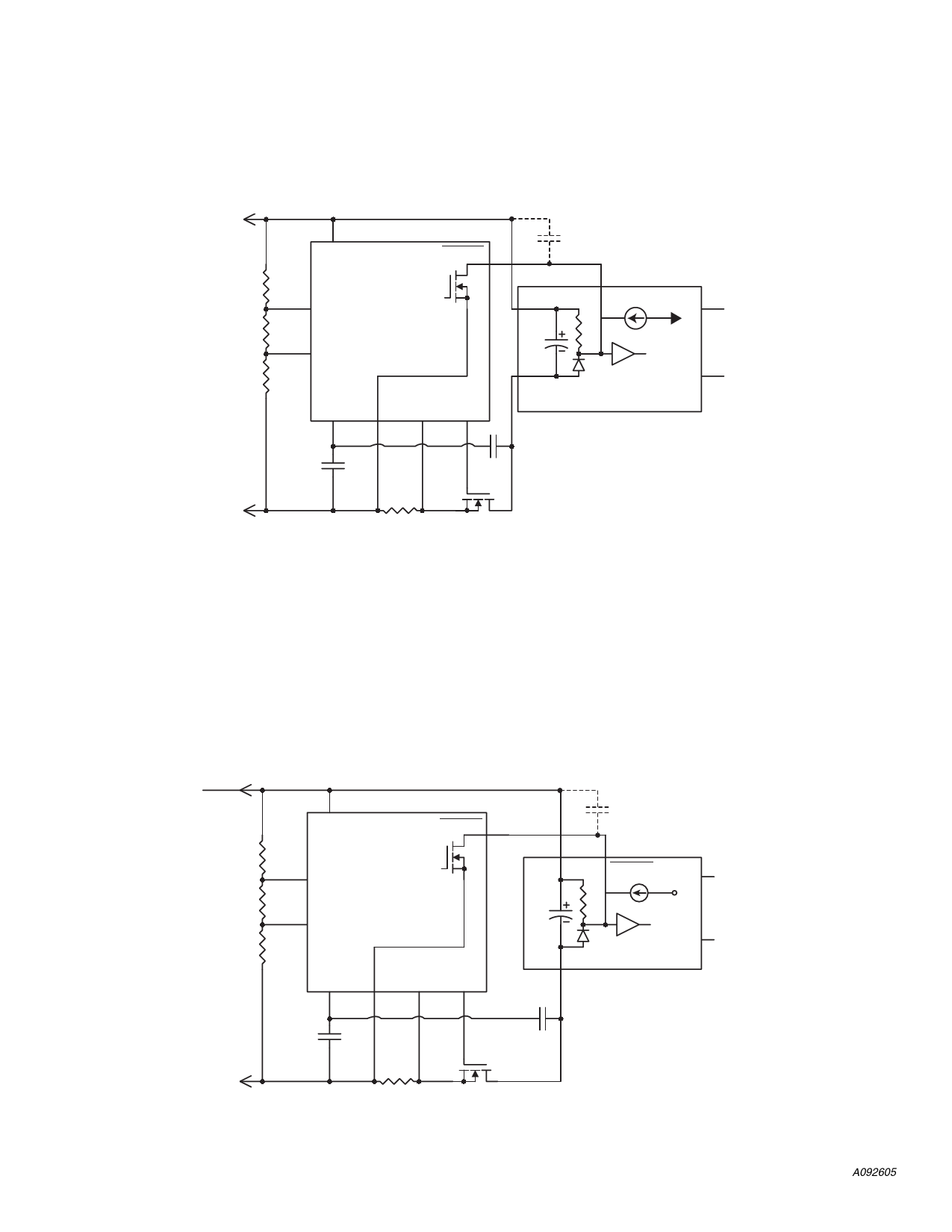
PWRGD Output
It is critical to have a detailed understanding of the ENABLE input
circuitry of the load (DC/DC PWM Converter) in order to make
the correct choice between the HV301 and HV311.
Many DC/DC PWM Converters reference their ENABLE inputs
to the negative input terminal. If the ENABLE input is active LOW
HV301/HV311
then the HV311 can be directly connected as shown below
(Application Circuit 1) since the open drain PWRGD output is
in a High-Z state until the external MOSFET is fully turned on and
the potential on the negative input of the converter is essentially
the same as the VEE pin of the HV311.
GND
R1
487kW
R2
6.81kW
R3
9.76kW
-48V
8
VDD
PWRGD
1
3 UV
2 OV
HV311
+
Cload
-
RAMP VEE
7
4
SENSE GATE
5
6
C1
10nF
R4
12.5mW
Q1
IRF530
Note: capacitor may be needed to slow PWRGD dv/dt if gate
oscillations around are observed when VIN is close to OVLO.
ENABLE
+5V
DC/DC
PWM
CONVERTER
COM
Application Circuit 1
However, if the DC/DC PWM Converter with the ENABLE input
circuit configuration was active HIGH, then the apparent choice
of the HV301 would result in the creation of a current path
through the protective diode clamp of the ENABLE input and the
PWRGD output MOSFET of the HV301. For this situation the
HV311 should be used as shown below in Application Circuit
2.
In some applications the PWRGD signal is used to activate load
circuitry on the isolated output side of the DC/DC PWM Con-
verter. In this situation an optocoupler is needed to provide the
required isolation as shown below in Application Circuit 3.
GND
R1
487kW
R2
6.81kW
R3
9.76kW
8
VDD
PWRGD
1
3 UV
2 OV
HV311
RAMP VEE
7
4
SENSE GATE
5
6
-48V
C1
10nF
R4
12.5mW
Q1
IRF530
Note: capacitor may be needed to slow PWRGD dv/dt if gate
oscillations around are observed when VIN is close to OVLO.
10
+
Cload
-
ENABLE
+5V
DC/DC
PWM
CONVERTER
COM
Application Circuit 2
A092605
Share Link: 