HV57009PG-G(2007) 데이터 시트보기 (PDF) - Supertex Inc
부품명
상세내역
제조사
HV57009PG-G
(Rev.:2007)
(Rev.:2007)
Supertex Inc

HV57009PG-G Datasheet PDF : 8 Pages
| |||
HV57009
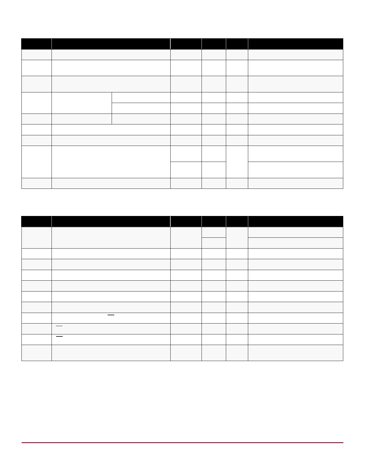
DC Electrical Characteristics (All voltages are referenced to VSS, VSS = 0, TA = 25OC)
Symbol Parameter
Min
Max Units Conditions
IDD
VDD supply current
INN
High voltage supply current
IDDQ
Quiescent VDD supply current
VOH High level output
Data Out
HVOUT
VOL
Low level output
Data Out
IIH
High-level logic input current
IIL
Low-level logic input current
ICS
High output source current
-
15
-
-10
-
VDD - 0.5V
+1.0
-
-
-
-
100
-
VDD
+0.5
1.0
-1.0
-2.0
-0.1
-
mA VDD = VDD max, fCLK = 8.0MHz
µA
Outputs off, HVOUT = -85V
(total of all outputs)
µA
All inputs = VDD,
except +IN = VSS = GND
V IO = -100µA
V IO = -2.0mA
V IO = 100µA
µA VIH = VDD
µA VIL = 0V
mA
VREF = 2.0V, REXT = 1K,
see Figures 1a and 1b
mA
VREF = 0.1V, REXT = 1K,
see Figures 1a and 1b
ΔICS HV output source current for IREF = 2.0mA
-
Note:
Current going out of the chip is considered negative.
10
% VREF = 2.0V, REXT = 1K
AC Electrical Characteristics (Logic signal inputs and data inputs have tr, tf ≤ 5ns [10% and 90% points] for measurements)
Symbol Parameter
Min
Max Units Conditions
fCLK
Clock frequency
8.0
Per register
DC
MHz
4.5
When cascading devices
tWL, tWH
tSU
tH
tON, tOFF
tDHL
tDLH
tDLE
tWLE
tSLE
tr, tf
Clock width high or low
Data set-up time before clock rises
Data hold time after clock rises
Time from latch enable to HVOUT
Delay time clock to data high to low
Delay time clock to data low to high
Delay time clock to LE low to high
LE pulse width
LE set-up time before clock rises
Max. allowable clock rise and fall time
(10% and 90% points)
62
-
ns ---
20
-
ns ---
15
-
ns ---
-
500
ns CL = 15pF
-
150
ns CL = 15pF
-
150
ns CL = 15pF
45
-
ns ---
25
-
ns ---
0
-
ns ---
-
100
ns ---
3
Share Link: