HV623PG 데이터 시트보기 (PDF) - Supertex Inc
부품명
상세내역
제조사
HV623PG Datasheet PDF : 10 Pages
| |||
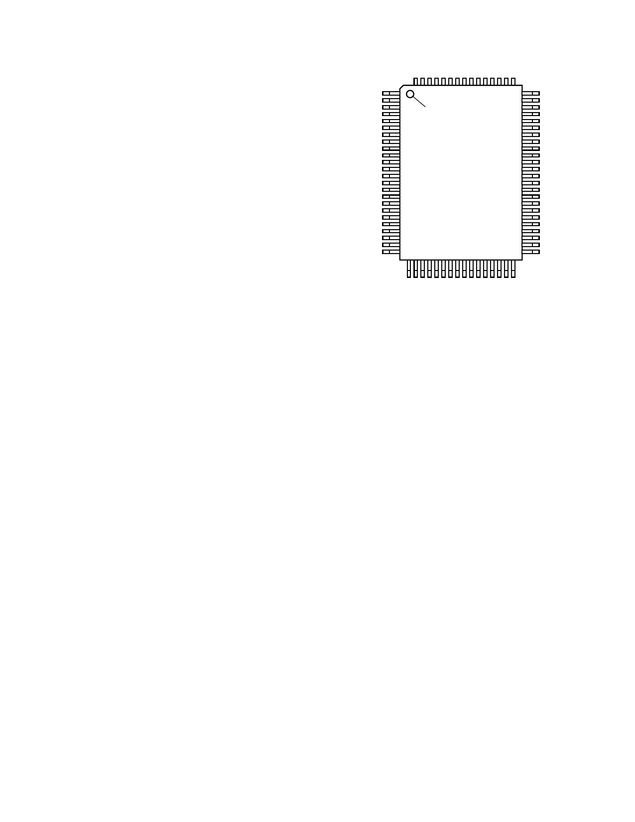
Pin Configuration
64-Pin PG Package
Pin Function
1
HVOUT 1
2
HVOUT 2
3
HVOUT 3
4
HVOUT 4
5
HVOUT 5
6
HVOUT 6
7
HVOUT 7
8
HVOUT 8
9
HVOUT 9
10 HVOUT 10
11 HVOUT 11
12 HVOUT 12
13 HVOUT 13
14 HVOUT 14
15 HVOUT 15
16 HVOUT 16
17 HVGND
18 VR
19 VPP
20 N/C
21 VDD (Analog)*
22 CSI
Pin Function
Pin Function
23 N/C
45 VPP
24 VCTL
46 N/C
25 RCTL
47 VR
26 SC (Shift Clock) 48 HVGND
27 LVGND
49 HVOUT 17
28 DIR
50 HVOUT 18
29 VDD (Digital)* 51 HVOUT 19
30 D7
52 HVOUT 20
31 D6
53 HVOUT 21
32 D5
54 HVOUT 22
33 D4
55 HVOUT 23
34 D3
56 HVOUT 24
35 D2
57 HVOUT 25
36 D1
58 HVOUT 26
37 N/C
59 HVOUT 27
38 LVGND
60 HVOUT 28
39 N/C
61 HVOUT 29
40 LC (Load Count) 62 HVOUT 30
41 N/C
63 HVOUT 31
42 CC (Count Clock) 64 HVOUT 32
43 CSO
44 N/C
* Analog VDD and digital VDD may be connected
separately for better noise immunity.
Package Outlines
1
Index
HV623
64
top view
24
41
25
40
3-Sided Plastic QFP 64-pin Gullwing Package
Theory of Operation
The HV623 has two primary functions:
1) Loading data from the data bus and,
2) Gray-shade conversion
(converting latched data to output voltages).
Since the device was developed initially for flat panel displays, the
operation will be described in terms that pertain to that technol-
ogy. As shown by the Typical Drive Scheme, several HV623
packages are mounted at the top and bottom of a display panel.
Data exists on a 7-bit bus (adjacent PC board traces) at top and
bottom. The D1 through D7 inputs of each chip take data from the
bus when either a CSI or CSO pulse is present at the chip. These
pulses therefore act as a combination CHIP SELECT and LOCA-
TION STROBE. Because of the way the chip HVOUT pins are
sequenced, data on the bus at the bottom of the display panel will
be entered into the left-most chip as HVOUT1, HVOUT2, etc. up to
HVOUT32. The CSI pulse will accomplish this with DIR = High.
Loading Data from Data Bus
Here is the full data-entry sequence:
1) The microcontroller puts data on the bus (7 bits)
2) To enter the data into the 32 sets of 7 latches on the first chip,
the shift clock rises. This positive transition is combined with
the CSI pulse and is generated only once to strobe the data into
the first set of latches. (These latches eventually send data to
the HVOUT1). The data on the bus then changes, the shift clock
falls, and this negative transition is combined with the CSI
pulse, which is now propagated internally, to strobe the new
data into the next set of 7 latches (which will end up as
HVOUT2). This internal CSI pulse therefore runs at twice the
shift clock rate.
3) When the last set of 7 latches in the first chip has been loaded
(HVOUT32), the CSI pulse leaves chip 1 and enters chip 2. The
exit pin is called CSO and the chip 2 entry pin is CSI . For chips
at the top of the panel things are reversed: DIR is low, entry pins
are CSO and exit pins are CSI , because the data-into-latches
sequence is in descending order, HVOUT32 down to HVOUT1.
4) The buses may of course be separate, and data can be strobed
in on an interleaved basis, etc., but those complications will be
left to systems designers.
12-130
Share Link: 