HV440WG 데이터 시트보기 (PDF) - Supertex Inc
부품명
상세내역
제조사
HV440WG Datasheet PDF : 5 Pages
| |||
Electrical Characteristics
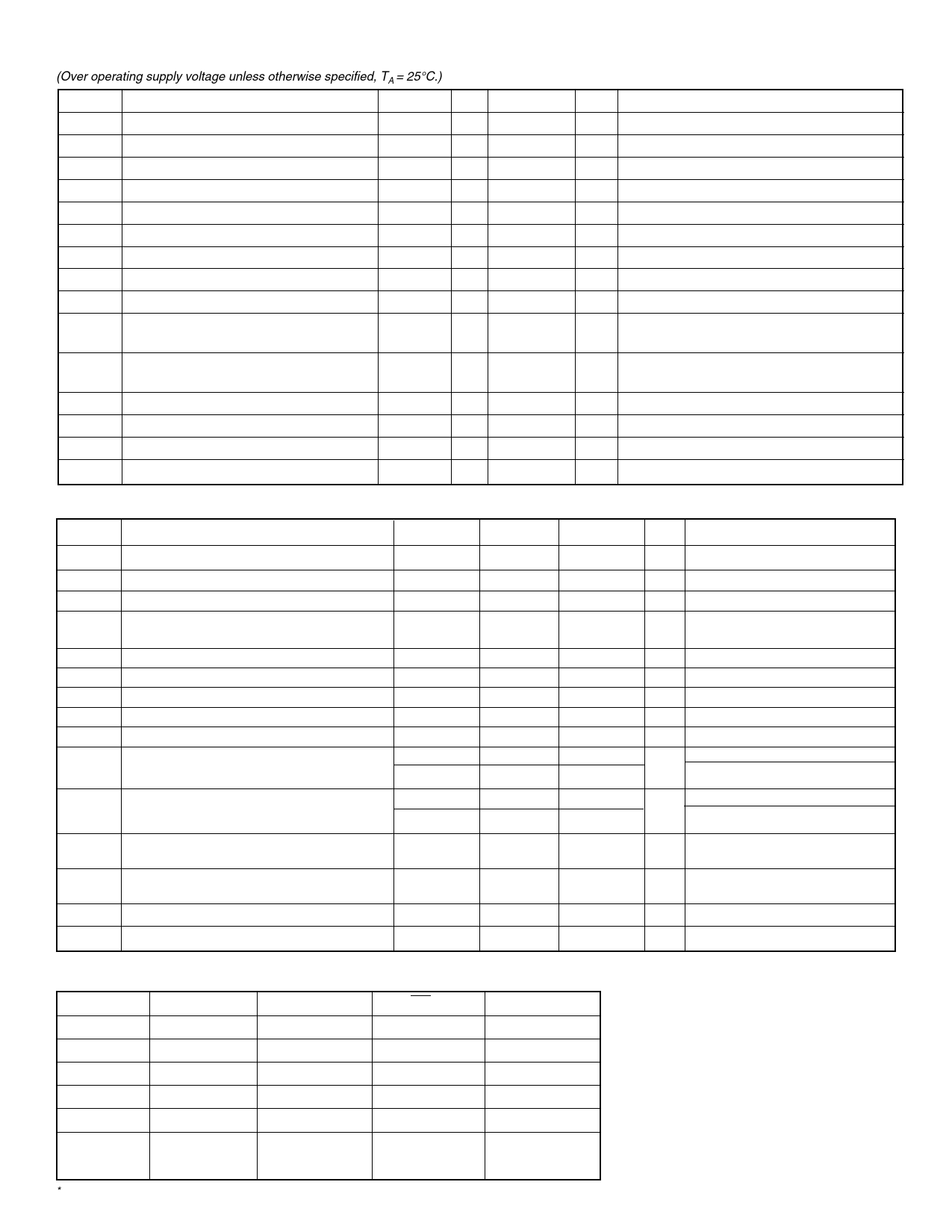
(Over operating supply voltage unless otherwise specified, TA = 25°C.)
Symbol Parameters
Min Typ
Max Unit
VPP1
VPP2
VNN1
VNN2
VDD
IPP1Q
INN1Q
IDDQ
IDDQ
IPP1
High voltage positive supply
15
110
V
Positive linear regulator output voltage
High voltage negative supply
Negative linear regulator output voltage
Logic supply voltage
VPP1 - 9.9
VPP1 - 220
VNN1 + 5.6
4.5
VPP1 -19.1 V
-110
V
VNN1 + 10.5 V
5.5
V
VPP1 quiescent current
VNN1 quiescent current
VDD1 quiescent current
VDD1 quiescent current
VPP1 operating current
250
400
µA
250
550
µA
150
µA
60
µA
1.7
mA
INN1
VNN1 operating current
1.9
mA
IDD
VDD operating current
IIL
Mode logic input low current
VIL
Logic input low voltage
VIH
Logic input high voltage
1.0
mA
25
µA
0
1.0
V
4.0
5.0
V
HV440
Conditions
TA = -40°C to +85°C
TA = -40°C to +85°C
TA = -40°C to +85°C
TA = -40°C to +85°C
TA = -40°C to +85°C
PIN = NIN = 0V, TA = -40°C to +85°C
PIN = NIN = 0V, TA = -40°C to +85°C
PIN = NIN = 0V Mode = 0
PIN = NIN = 0V Mode = 1
No load, VOUTP and VOUTN switching at
100KHz, TA = -40°C to +85°C
No load, VOUTP and VOUTN switching at
100KHz, TA = -40°C to +85°C
Mode = 0V
VDD = 5.0V
VDD = 5.0V
High Voltage Output
Symbol Parameters
Min
Typ
Max
Unit Conditions
RSOURCE VOUTP source resistance
IOUT = 100mA
RSINK VOUTP sink resistance
∆R/∆T Change in source/sink resistance
over temperature
60
80
Ω
60
80
Ω
0.33
Ω/°C
td(ON)
trise
td(OFF)
tfall
tdb
Vpsen
HVOUT delay time
HVOUT rise time
HVOUT delay time
HVOUT fall time
Logic deadband time
HVOUT current source sense voltage
150
ns
50
ns
200
ns
50
ns
200
ns
VPP1 -0.75 VPP1 -1.00 VPP1 - 1.25 V
VPP1 -0.67
VPP1 -1.31
Vnsen
tshortP
HVOUT current sink sense voltage
VNN1 + 0.75 VNN1 + 1.00 VNN1 + 1.25 V
VNN1 + 0.65
VNN1 + 1.33
HVOUT off time when current source sense
is activated
100
ns
tshortN
HVOUT off time when current sink sense
is activated
100
ns
tWHOUT Minimum pulse width for HVOUT at VPP1
500
ns
tWLOUT Minimum pulse width for HVOUT at VNN1
500
ns
IOUT = -100mA
TA = -40°C to +85°C
PIN = high to low, Mode = high
PIN = high to low
NIN = low to high, Mode = high
NIN = low to high
Mode = low
TA = -40°C to +85°C
TA = -40°C to +85°C
TA = -40°C to +85°C
TA = -40°C to +85°C
Truth Table
NIN
PIN
Mode
EN
L
L
H
L
L
H
H
L
H
L*
H
L
H
H
H
L
L
X
L
L
H
X
L
L
X
X
X
H
*This state will short VPP1 to VNN1 and should therefore be avoided.
HVOUT
VPP1
High Z
–
VNN1
V
NN1
VPP1
High Z
2
032105
Share Link: 