HV6810(2007) 데이터 시트보기 (PDF) - Supertex Inc
부품명
상세내역
제조사
HV6810 Datasheet PDF : 8 Pages
| |||
HV6810
Pin Descriptions
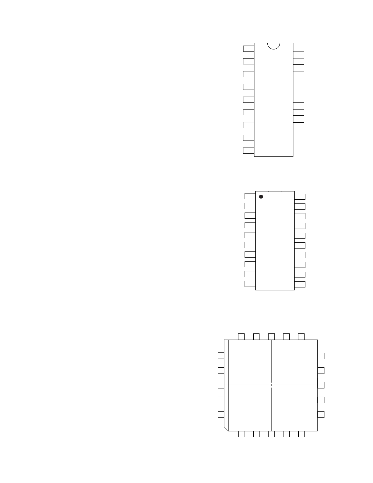
HV6810 20-J Lead PLCC (PJ)
Pin
Function
Description
1
Q8
2
Q7
High voltage output.
3
Q6
4
CLOCK
Input data are shifted into the data shift register on the thepostive edge of the
clock.
5
N/C
No connection.
6
VSS
Usually VSS = 0, ground connection.
7
VDD
Low voltage power supply.
When LE is high, data is transferred from data shift register to the Q output latch.
8
LE (STROBE)
When LE is low, data is latched into data latches and new data can be clocked into
the shift register.
9
Q5
10
Q4
11
Q3
High voltage output.
12
Q2
13
Q1
When blanking is low, all Q’s are forced to a high state, regardless of data in each
14
BLANKING
channel. When OL is low, all Q’s are forced to a low state, regardless of data in
each channel.
15
DATA IN
Input data for the input shift register.
16
N/C
No connection.
17
VBB
High voltage power supply.
18
SERIAL DATA OUT Output data from the shift register.
19
Q10
High voltage output.
20
Q9
5
Share Link: 