HV6810PJ-G 데이터 시트보기 (PDF) - Supertex Inc
부품명
상세내역
제조사
HV6810PJ-G Datasheet PDF : 8 Pages
| |||
HV6810
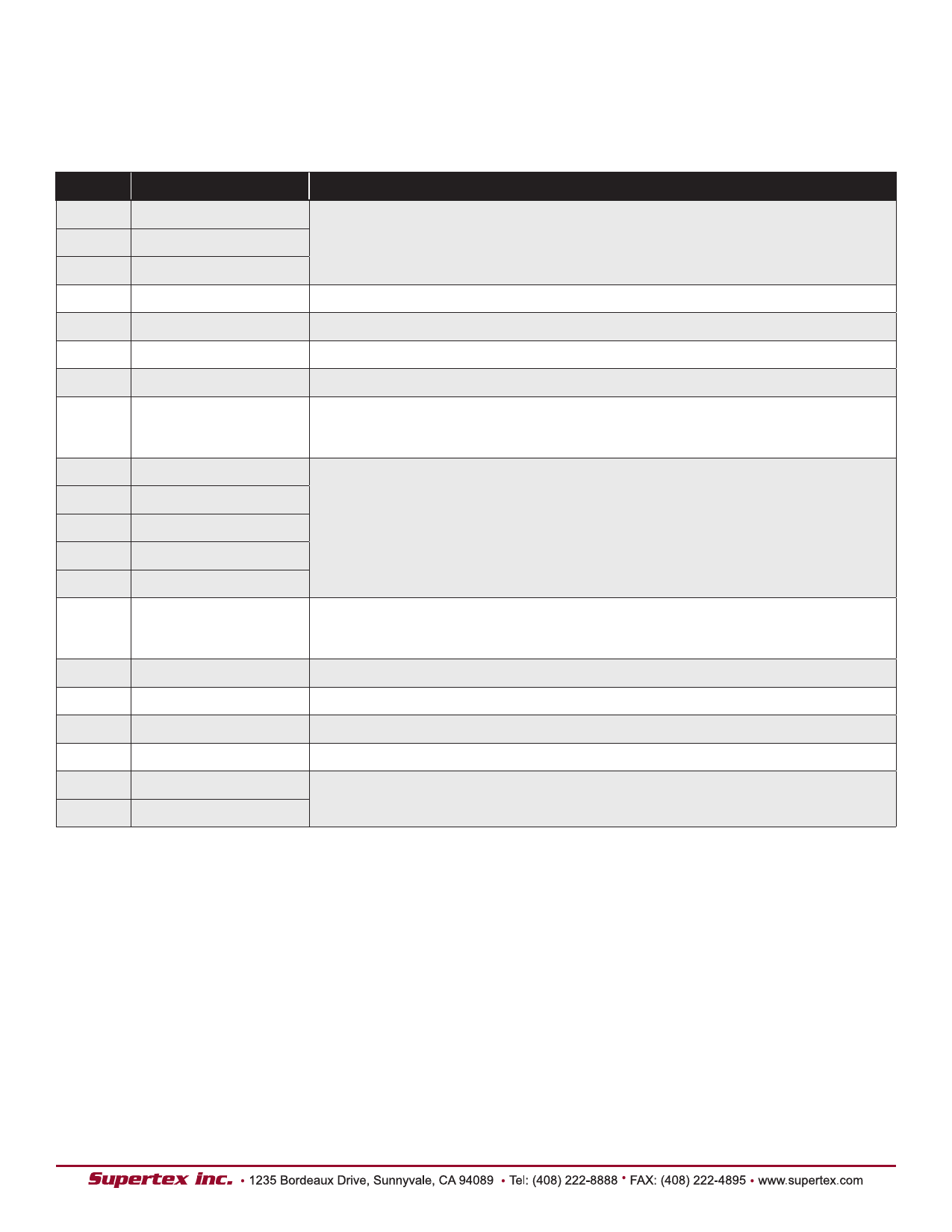
Pin Descriptions
HV6810 20-Lead SOW (WG)
Pin
Function
1
Q8
2
Q7
High voltage output.
3
Q6
4
CLOCK
Input data are shifted into the data shift register on the thepostive edge of the clock.
5
VSS
Usually VSS = 0, ground connection.
6
N/C
No connection.
7
VDD
Low voltage power supply.
When LE is high, data is transferred from data shift register to the Q output latch.
8
LE (STROBE)
When LE is low, data is latched into data latches and new data can be clocked into
the shift register
9
Q5
10
Q4
11
Q3
High voltage output.
12
Q2
13
Q1
When blanking is low, all Q’s are forced to a high state, regardless of data in each
14
BLANKING
channel. When OL is low, all Q’s are forced to a low state, regardless of data in each
channel.
15
DATA IN
Input data for the input shift register.
16
VBB
High voltage power supply.
17
SERIAL DATA OUT Output data from the shift register.
18
N/C
No connection.
19
Q10
High voltage output.
20
Q9
6
Share Link: 