HV9608TS 데이터 시트보기 (PDF) - Supertex Inc
부품명
상세내역
제조사
HV9608TS Datasheet PDF : 6 Pages
| |||
SLOPE COMPENSATION
The HV9608 PWM controller uses an internal slope compensation
scheme that is externally programmable by appropriately selecting
two resistors RSC1 and RCS2. The slope compensation ramp
generated at the CS pin can be calculated as:
[ ] [ ] mSC
V / µs
= 5.7 ⋅10−6 ⋅ FOSC
Hz
⋅ RSC2
R SC1
RSC1 must be selected greater than 5 kΩ.
When a current sense RC filter is needed at the SC pin, the value
of RCS2 will be dictated by the filter capacitor and the corner
frequency of the filter. The filter capacitor externally connected to
the CS pin is discharged prior to each switching cycle. It is not
recommended to use a capacitor larger than 220pF for this reason.
GATE DRIVE OUTPUTS
The HV9608 provides two gate-drive outputs that are configured
for driving a low-side clamp DC-DC converter, having a main
switching N-channel MOSFET (Q1) and an auxiliary active clamp
P-channel MOSFET (Q2). The GATE output is designed to drive
the main N-channel MOSFET Q1, while the AGATE output drives
Q2 via a negative output charge pump circuit C4, D1, R5. Delays
between the leading and the trailing edges of the gate drive
outputs can be programmed using external resistors RDT1 and RDT2
connected to the DT1 and DT2 pins, respectively. The values of
RDT1 and RDT2 can be calculated according to the following
equations:
[ ] R DT1 = 8 ×10¹¹ ⋅ d1 s ,
[ ] R DT2 = 8×10¹¹ ⋅ d2 s ,
HV9608
where d1 is the leading edge delay, d2 is the trailing edge delay.
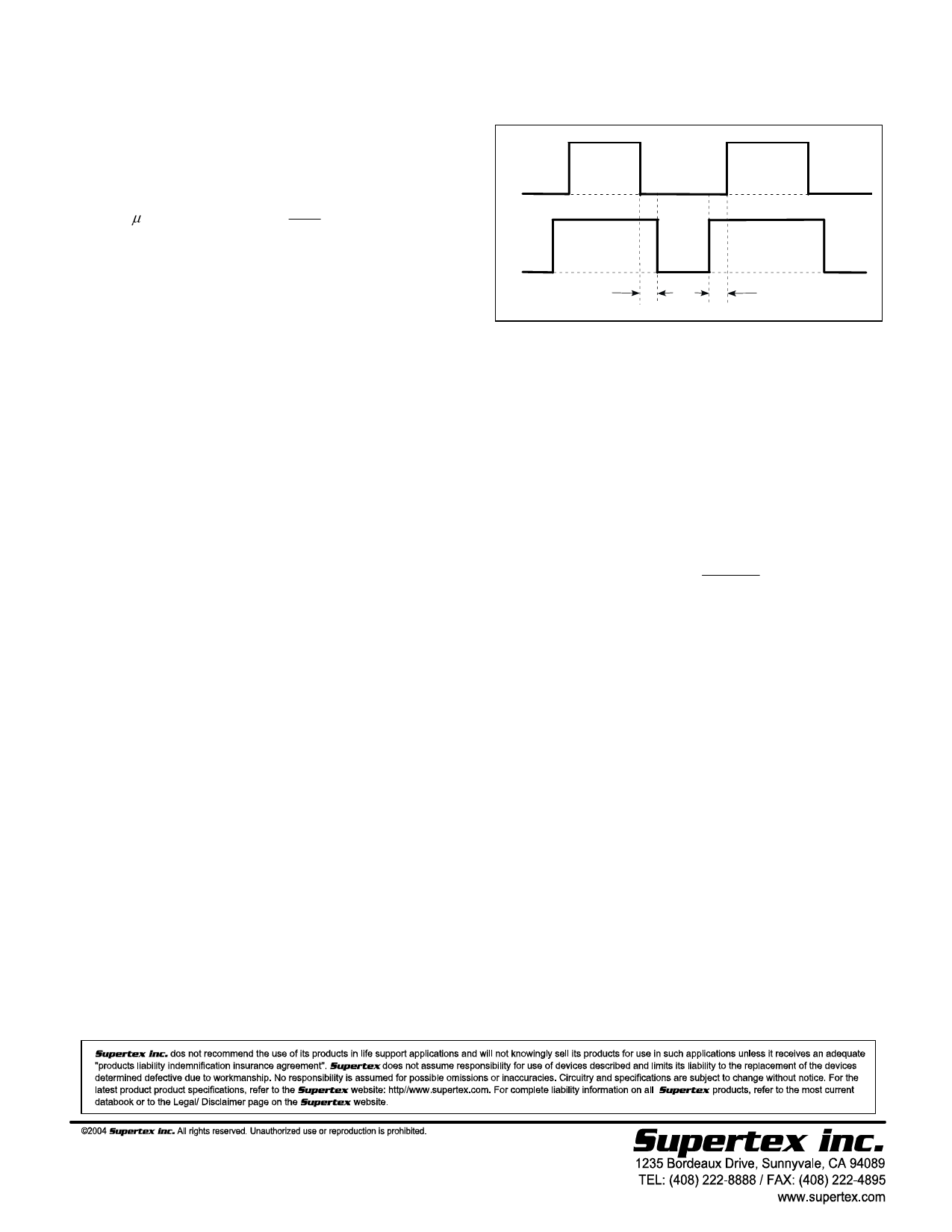
(Refer to Fig. 2.)
GATE
AGATE
d1
d2
Figure 2. Gate Drive Output timing diagram.
VOLT-SECOND CLAMP
The duty cycle of the active DC-DC converter may become very
large during load transients. This condition may cause saturation of
the power transformer or excessive voltage stress at the clamp
capacitor C3, potentially damaging for all switching devices. In
order to prevent this condition, the HV9608 includes a volt-second
clamp circuit that can be programmed to limit the maximum duty
cycle of the PWM controller, which is inversely proportional to the
input voltage of the DC-DC converter. The maximum duty cycle
DMAX is set by merely connecting a single resistor RVS between the
positive input terminal of the converter and the VS pin. RVS can be
calculated with the following equation.
( ) RVS
= 1.72×10⁹ ⋅
VIN [V ] − 0.7
⋅
⎛
⎜⎜⎝
DMAX
[ FOSC Hz
]
+
d1
[
s]
+
2
×10−8
⎞
⎟⎟⎠
Doc. #: DSFP-HV9608
6
A122104
A122104
Share Link: 