HV9801ANG-G(2011) 데이터 시트보기 (PDF) - Supertex Inc
부품명
상세내역
제조사
HV9801ANG-G Datasheet PDF : 9 Pages
| |||
HV9801A
Ordering Information
Device
HV9801A
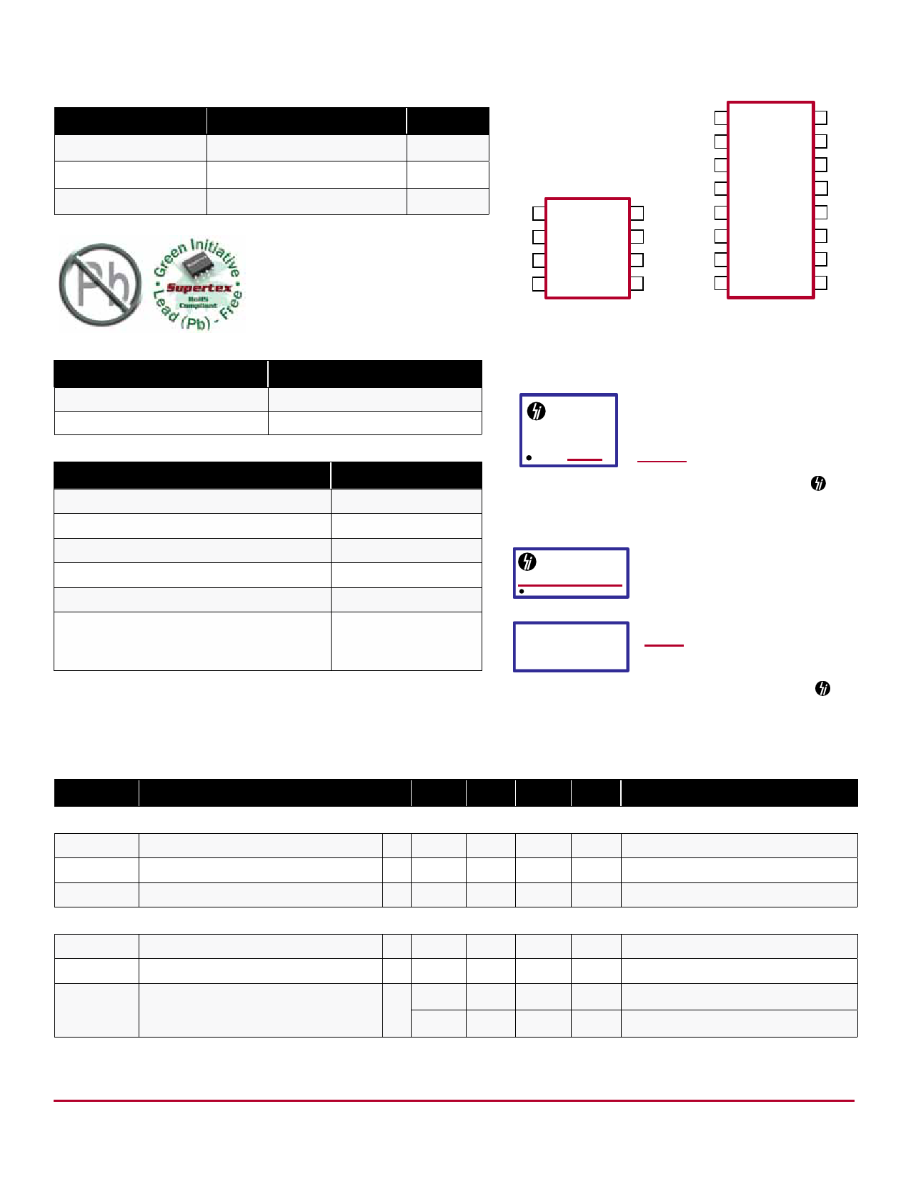
Package Options
8-Lead SOIC
4.90x3.90mm body
1.75mm height (max)
1.27mm pitch
16-Lead SOIC
9.90x3.90mm body
1.75mm height (max)
1.27mm pitch
HV9801ALG-G
HV9801ANG-G
-G indicates package is RoHS compliant (‘Green’)
Pin Description
VIN 1
DNC 2
DNC 3
CS 4
VIN 1
8 RT
GND 5
CS 2
7 DNC DNC 6
GND 3
6 VDD DNC 7
GATE 4
5 DNC GATE 8
16 DNC
15 DNC
14 RT
13 DNC
12 VDD
11 DNC
10 DNC
9 DNC
8-Lead SOIC (LG)
16-Lead SOIC (NG)
Caution! DNC means Do Not Connect!
Absolute Maximum Ratings
Parameter
Value
VVIN
VVDD
VCS, VLD, VPWMD, VGATE
Junction temperature range
470V
12V
-0.3V to (VVDD +0.3V)
-40°C to +150°C
Product Marking
YWW
9801A
LLLL
Y = Last Digit of Year Sealed
WW = Week Sealed
L = Lot Number
= “Green” Packaging
Package may or may not include the following marks: Si or
8-Lead SOIC (LG)
Storage temperature range
-65°C to +150°C
Continuous power dissipation (TA = +25°C)
8-Lead SOIC
16-Lead SOIC
650mW
1000mW
Stresses beyond those listed under “Absolute Maximum Ratings” may cause
permanent damage to the device. These are stress ratings only, and functional
operation of the device at these or any other conditions beyond those indicated in
the operational sections of the specifications is not implied. Exposure to absolute
maximum rating conditions for extended periods may affect device reliability.
Top Marking
HV9801ANG
YWW LLLLLLLL
Bottom Marking
CCCCCCCCC AAA
Y = Last Digit of Year Sealed
WW = Week Sealed
L = Lot Number
C = Country of Origin*
A = Assembler ID*
= “Green” Packaging
*May be part of top marking
Package may or may not include the following marks: Si or
16-Lead SOIC (NG)
Electrical Characteristics (Specifications are at TA = 25°C, VVIN = 15V unless otherwise noted)
Sym Description
Min Typ Max Unit Conditions
Input
VVIN
Input voltage
IVIN
Input current
IVIN,OT Supply current, OTP shutdown
VDD Regulator
T 15
--
G-
-
450
V ---
1
2
mA ---
- 500 μA ---
VUVLO Undervoltage lockout threshold
T 6.45 6.70 7.10 V
ΔVUVLO Undervoltage lockout hysteresis
-
-
500
-
mV
IUVLO
Maximum input current, limited by
UVLO
G
3.5
1.5
-
-
-
mA
-
mA
Notes:
G Not production tested; guaranteed by design or characterization.
T Specifications apply over the full operating ambient temperature range of -40°C < TA < +125°C.
VVIN rising
VVIN falling
TA = 25°C
TA = 125°C
Supertex inc. ● 1235 Bordeaux Drive, Sunnyvale, CA 94089 ● Tel: 408-222-8888 ● www.supertex.com
2
Share Link: 