HV9911NG-G 데이터 시트보기 (PDF) - Supertex Inc
부품명
상세내역
제조사
HV9911NG-G Datasheet PDF : 9 Pages
| |||
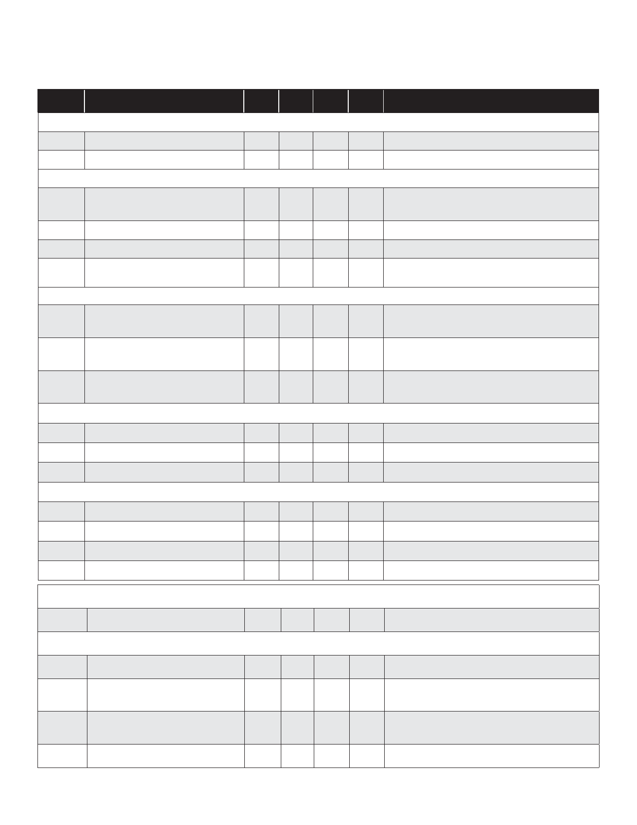
HV9911
Electrical Characteristics
(Over recommended operating conditions, VIN = 24V, TA = 25°C, unless otherwise specified)
Symbol Parameter
Min Typ Max Units Conditions
Input
VINDC
Input DC supply voltage range*
IINSD
Shut-Down mode supply current*
Internal Regulator
9
-
250
V DC input voltage
-
1.0 1.5 mA PWM_D connected to GND, VIN = 24V
V
Internally regulated voltage*
DD
7.25 7.75 8.25
V
VIN = 9–250V, IDD(ext) = 0,
PWMD connected to GND
UVLO VDD undervoltage lockout threshold
∆UVLO VDD undervoltage lockout hysteresis
VDD(ext)
Steady State External Voltage
which can applied at the V pin1
DD
Reference
6.65
-
-
6.90
500
-
7.20
-
12
V VDD rising
mV ---
V ---
V
REF pin voltage*
REF
1.225 1.25 1.275
V
REF bypassed with a 0.1µF capacitor to GND;
IREF= 0; VDD = 7.75V; PWMD = GND
VREFLINE Line regulation of reference voltage
0
-
20
mV
REF bypassed with a 0.1µF capacitor to GND;
IREF = 0; VDD = 7.25 – 12V; PWMD = GND
VREFLOAD
Load regulation of reference
voltage
0
-
10
mV
REF bypassed with a 0.1µF capacitor to GND;
IREF = 0 - 500µA; PWMD = GND
PWM Dimming
VPWMD(lo)
VPWMD(hi)
RPWMD
GATE
PWMD input low voltage*
PWMD input high voltage*
PWMD pull-down resistance
-
-
0.80
V VDD = 7.25V – 12V
2.0
-
-
V VDD = 7.25V – 12V
50
100 150
kΩ VPWMD = 5.0V
ISOURCE
ISINK
TRISE
TFALL
GATE short circuit current
GATE sinking current
GATE output rise time
GATE output fall time
0.2
-
-
A
VGATE = 0V; VDD = 7.75V
0.4
-
-
A VGATE = 7.75V ; VDD = 7.75V
-
50
85
ns CGATE = 1nF; VDD = 7.75V
-
25
45
ns CGATE = 1nF; VDD = 7.75V
Over Voltage Protection
VOVP
IC Shut down voltage*
Current Sense
1.215 1.25 1.285 V VDD = 7.25 – 12V ; OVP rising
TBLANK
Leading Edge Blanking
100
-
375 ns ---
TDELAY1
Delay to Output of OP comparator
-
-
180
ns
OP = VDD ; CLIM = REF;
CSENSE = 0 to 600mV step
TDELAY2
Delay to Output of CLIMIT
comparator
-
-
180
ns
OP = VDD ; CLIM = 300mV ;
CSENSE = 0 to 400mV step
VOFFSET
Comparator Offset voltage
-10
-
10 mV ---
NR011206
3
Share Link: 