ICS309 데이터 시트보기 (PDF) - Integrated Circuit Systems
부품명
상세내역
제조사
ICS309 Datasheet PDF : 8 Pages
| |||
ICS309
SERIAL PROGRAMMABLE TRIPLE PLL SS VERSACLOCK SYNTHESIZER
Configuring the ICS309
Initial State: The ICS309 may be configured to have up to 9 frequency outputs, utilizing the 4 on-board
PLLs and spread spectrum circuitry. Unprogrammed, the part has the following outputs, related to the
reference input clock:
Default Outputs
Output
Frequency
Clocks 1 - 9 (Pins 4, 7-14)
Reference Output
The STROBE pin must have an external 250 kOhm pull-up resistor to acheive the Initial State.
The input crystal range for the ICS309 is 5 MHz to 27 MHz.
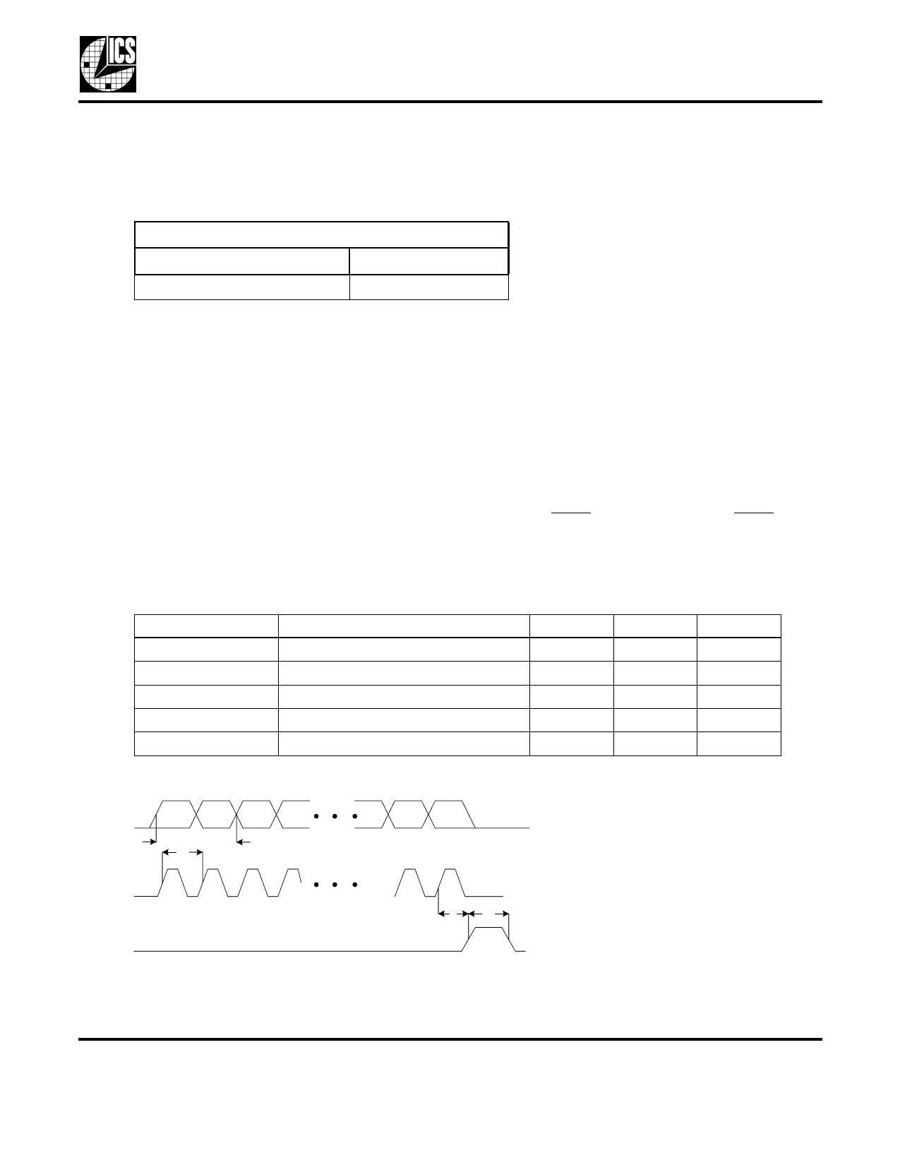
The ICS309 can be programmed to set the output functions and frequencies. 160 data bits generated by
the VersaClockTM software are written in DATA pin in this order: MSB (left most bit) first.
As show in Figure 2, after these 160 bits are clocked into the ICS309, taking STROBE high will send this
data to the internal latch and the CLK output will lock within 10 ms.
Note: STROBE utilizes a transparent latch that is latched when in the high state. If STROBE is in the high
state and SCLK is pulsed, DATA is clocked directly to the internal latch and the output conditions will
change accordingly. Although this will not damage the ICS309, it is recommended that STROBE be kept
low while DATA is being clocked into the ICS309 in order to avoid unintended changes on the output clocks.
All outputs may be turned off during initialization by bringing the PDTS pin to Ground. When PDTS is
brought high, after the Strobe pin in brought high, the programmed output frequencies will be available.
AC Parameters for Writing to the ICS309
Parameter
tSETUP
tHOLD
tW
tS
Condition
Setup time
Hold time after SCLK
Data wait time
Strobe pulse width
SCLK Frequency
Min.
10
10
10
40
Max.
30
Units
ns
ns
ns
ns
MHz
DATA Bit160 Bit159 Bit158
tsetup
thold
Bit3 Bit2 Bit1
SCLK
STROBE
tw
ts
Figure 2. Timing Diagram for Programming the ICS309
MDS 309 G
3
Revision 122704
Integrated Circuit Systems ● 525 Race Street, San Jose, CA 95126 ● tel (408) 297-1201 ● www.icst.com
Share Link: 