ICS309 데이터 시트보기 (PDF) - Integrated Circuit Systems
부품명
상세내역
제조사
ICS309 Datasheet PDF : 8 Pages
| |||

ICS309
SERIAL PROGRAMMABLE TRIPLE PLL SS VERSACLOCK SYNTHESIZER
Spread Spectrum Modulation
The ICS309 utilizes frequency modulation (FM) to
distribute energy over a range of frequencies. By
modulating the output clock frequencies, the device
effectively lowers energy across a broader range of
frequencies; thus, lowering a system’s
electro-magnetic interference (EMI). The modulation
rate is the time from transitioning from a minimum
frequency to a maximum frequency and then back to
the minimum.
Spread Spectrum Modulation can be applied as either
“center spread” or “down spread”. During center spread
modulation, the deviation from the target frequency is
equal in the positive and negative directions. The
effective average frequency is equal to the target
frequency. In applications where the clock is driving a
component with a maximum frequency rating, down
spread should be applied. In this case, the maximum
frequency, including modulation, is the target
frequency. The effective average frequency is less than
the target frequency.
The ICS309 operates in both center spread and down
spread modes. For center spread, the frequency can
be modulated between ±0.125% to ±2.0%. For down
spread, the frequency can be modulated between
-0.25% to -4.0%.
Both output frequency banks will utilize identical spread
spectrum percentage deviations and modulation rates,
if a common VCO frequency can be identified.
Spread Spectrum Modulation Rate
The spread spectrum modulation frequency applied to
the output clock frequency may occur at a variety of
rates. For applications requiring the driving of
“down-circuit” PLLs, Zero Delay Buffers, or those
adhering to PCI standards, the spread spectrum
modulation rate should be set to 30-33 kHz. For other
applications, a 120 kHz modulation option is available.
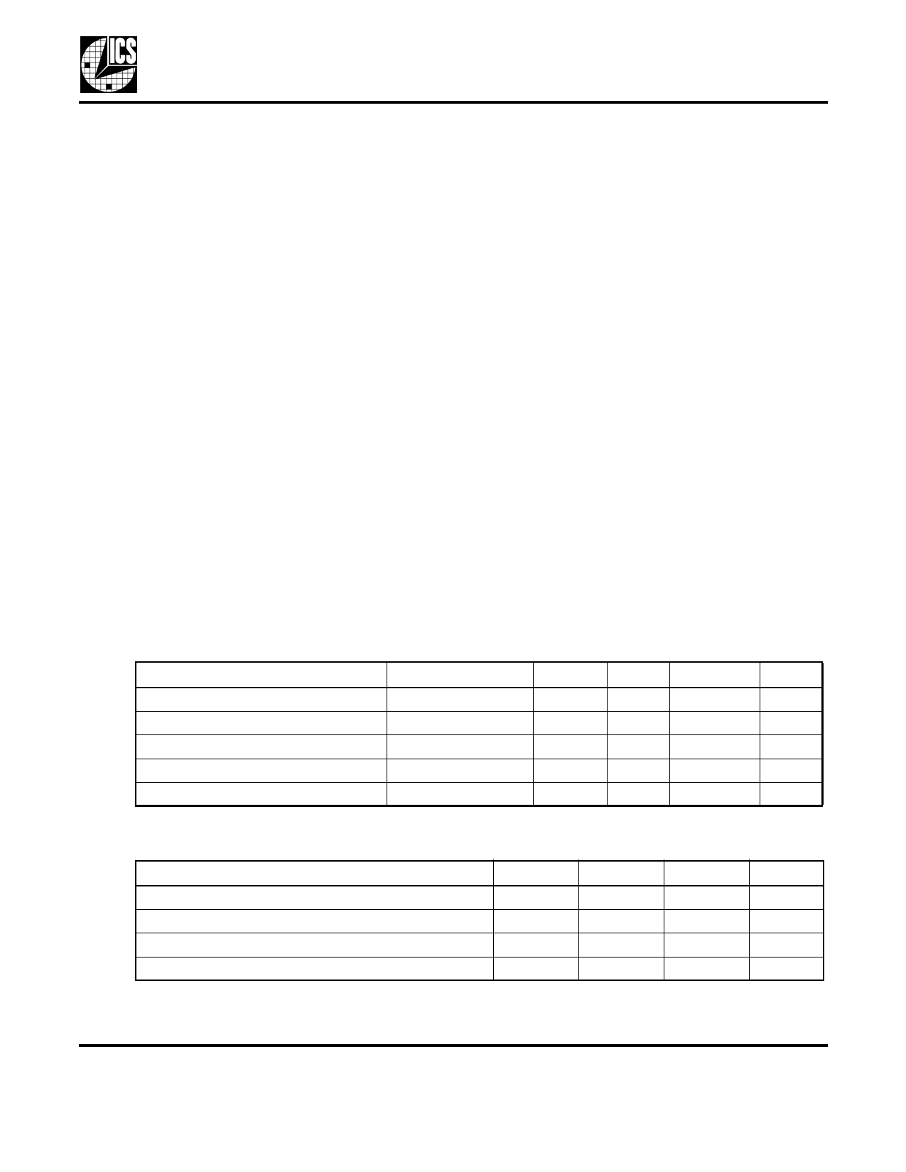
Absolute Maximum Ratings
Stresses above the ratings listed below can cause permanent damage to the ICS309. These ratings, which
are standard values for ICS commercially rated parts, are stress ratings only. Functional operation of the
device at these or any other conditions above those indicated in the operational sections of the
specifications is not implied. Exposure to absolute maximum rating conditions for extended periods can
affect product reliability. Electrical parameters are guaranteed only over the recommended operating
temperature range.
Parameter
Condition
Min. Typ. Max. Units
Supply Voltage, VDD
Referenced to GND
7
V
Inputs
Referenced to GND -0.5
VDD+ 0.5
V
Clock Outputs
Referenced to GND -0.5
VDD+ 0.5
V
Storage Temperature
-65
150
°C
Soldering Temperature
Max 10 seconds
260
°C
Recommended Operation Conditions
Parameter
Ambient Operating Temperature
Ambient Operating Temperature (ICS309RI)
Power Supply Voltage (measured in respect to GND)
Power Supply Ramp Time
Min.
0
-40
+3.0
Typ.
Max.
+70
+85
+3.6
4
Units
°C
°C
V
ms
MDS 309 G
5
Revision 122704
Integrated Circuit Systems ● 525 Race Street, San Jose, CA 95126 ● tel (408) 297-1201 ● www.icst.com