ICS93701 데이터 시트보기 (PDF) - Integrated Circuit Systems
부품명
상세내역
제조사
ICS93701 Datasheet PDF : 9 Pages
| |||
ICS9370 1
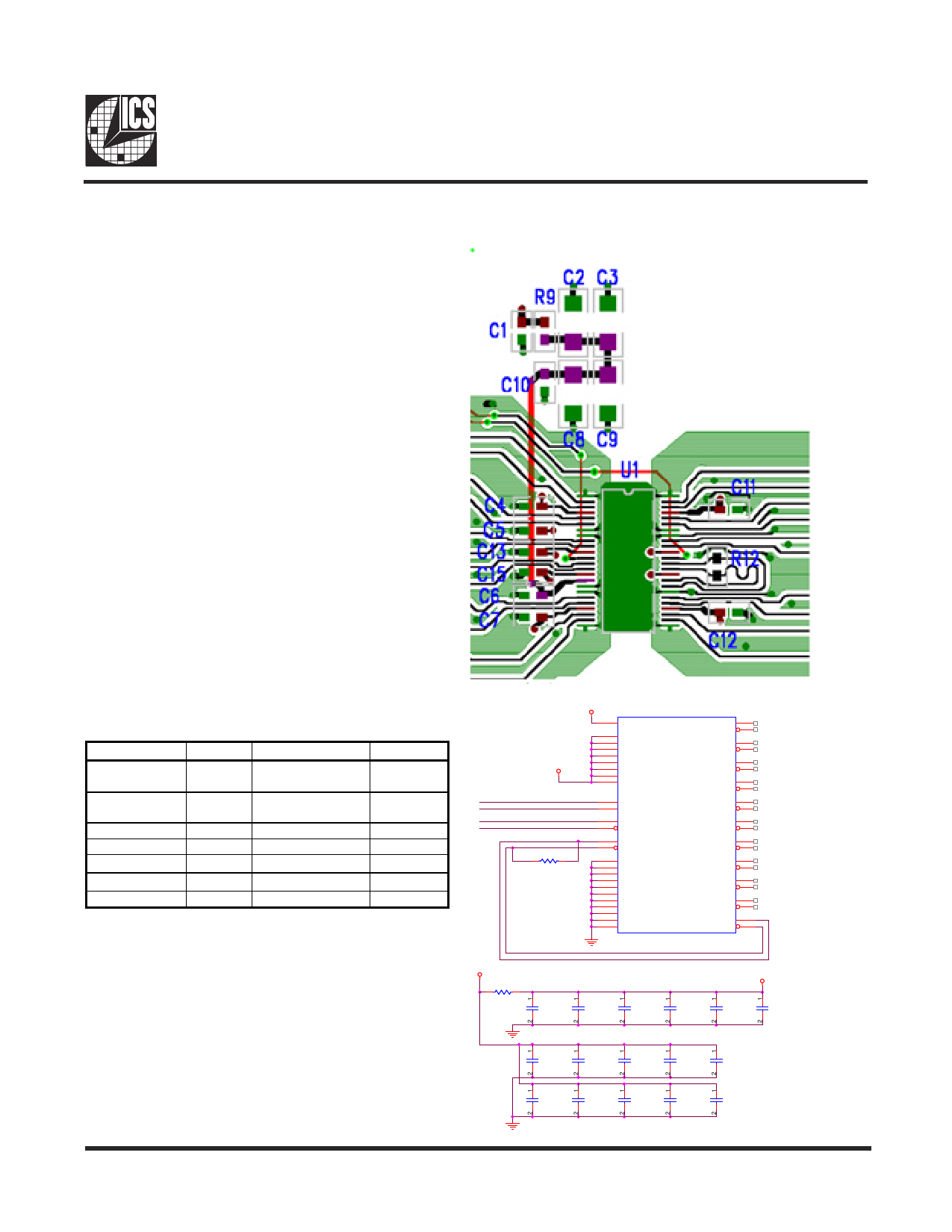
Recommended Layout for the ICS93701
General Layout Precautions:
Use copper flooded ground on the top signal layer under the
clock buffer The area under U1 on the right is an example.
Flood over the ground vias.
1) Use power vias for power and ground. Vias 20 mil or
larger in diameter have lower high frequency impedance.
Vias for signals may be minimum drill size.
2) Make all power and ground traces are as wide as the via
pad for lower inductance.
3) VAA for pin 16 has a low pass RC filter to decouple the
digital and analog supplies. The 4.7uF capacitors may be
replaced with a single low ESR device with the same
total capacitance. VAA is routed on a outside signal
layer. Do not cut a power or ground plane and route in it.
4) Notice that ground vias are never shared.
5) When ever possible, VCC (net V2P5 in the schematic)
pins have a decoupling capacitor. Power is always routed
from the plane connection via to the capacitor pad to the
VCC pin on the clock buffer. Moats or plane cuts are not
used to isolate power.
6) Differential mode clock output traces are routed:
a. With a ground trace between the pairs. Trace is
grounded on both ends.
b. Without a ground trace, clock pairs are routed with a
separation of at least 5 times the thickness of the
dielectric. If the dielectric thickness is 4.5 mil, the
trace separation is at least 18 mils.
Component Values:
Ref Desg. Value
C1,C4,C5, .01uF
C7,C11,C12
C2,C3,C8,
C9
4.7uF
C10
.22uF
C6
2200pF
R12
120 Ω
R9
4.7 Ω
U1
Description
CERAMIC MLC
CERAMIC MLC
CERAMIC MLC
CERAMIC MLC
ICS93701AG
Package
0603
1206
0603
0603
0603
0603
TSSOP48
V2P5
SCL
SDA
CLK_IN
CLK_IN#
FB_IN
FB_IN#
R12
1
120
2
V2A5
U1
16 AVDD
4
11
15
VDD
VDD
21
28
34
38
VDD
VDD
VDD
VDD
45
VDD
VDD
12
37
SCL
SDA
13
14
CLK_INT
CLK_INC
35
36
FB_INT
FB_INC
1
7
GND
8
18
24
25
GND
GND
GND
GND
31
41
42
48
17
GND
GND
GND
GND
GND
AGND
ICS93701
V2P5
R9
1
2
4.7
C2
4.7uF
V2A5
C3
4.7uF
C8
4.7uF
CLKT0
3
2
CLKC0
CLKT1
5
6
CLKC1
CLKT2
CLKC2
10
9
CLKT3
20
19
CLKC3
CLKT4
22
23
CLKC4
CLKT5
CLKC5
46
47
CLKT6
CLKC6
44
43
CLKT7
39
40
CLKC7
CLKT8
CLKC8
29
30
CLKT9
CLKC9
27
26
FB_OUTT
33
32
FB_OUTC
C9
4.7uF
V2A5
C10
.22uF
C6
.0022pF
0417B—10/29/02
C4
.01uF
C1
.01uF
C5
.01uF
C13
.01uF
C16
.01uF
C12
.01uF
C15
.01uF
C14
.01uF
C11
.01uF
C7
.01uF
8
Share Link: 