IDT49C460 데이터 시트보기 (PDF) - Integrated Device Technology
부품명
상세내역
제조사
IDT49C460 Datasheet PDF : 32 Pages
| |||
IDT49C460/A/B/C/D/E
32-BIT CMOS ERROR DETECTION AND CORRECTION UNIT
MILITARY AND COMMERCIAL TEMPERATURE RANGES
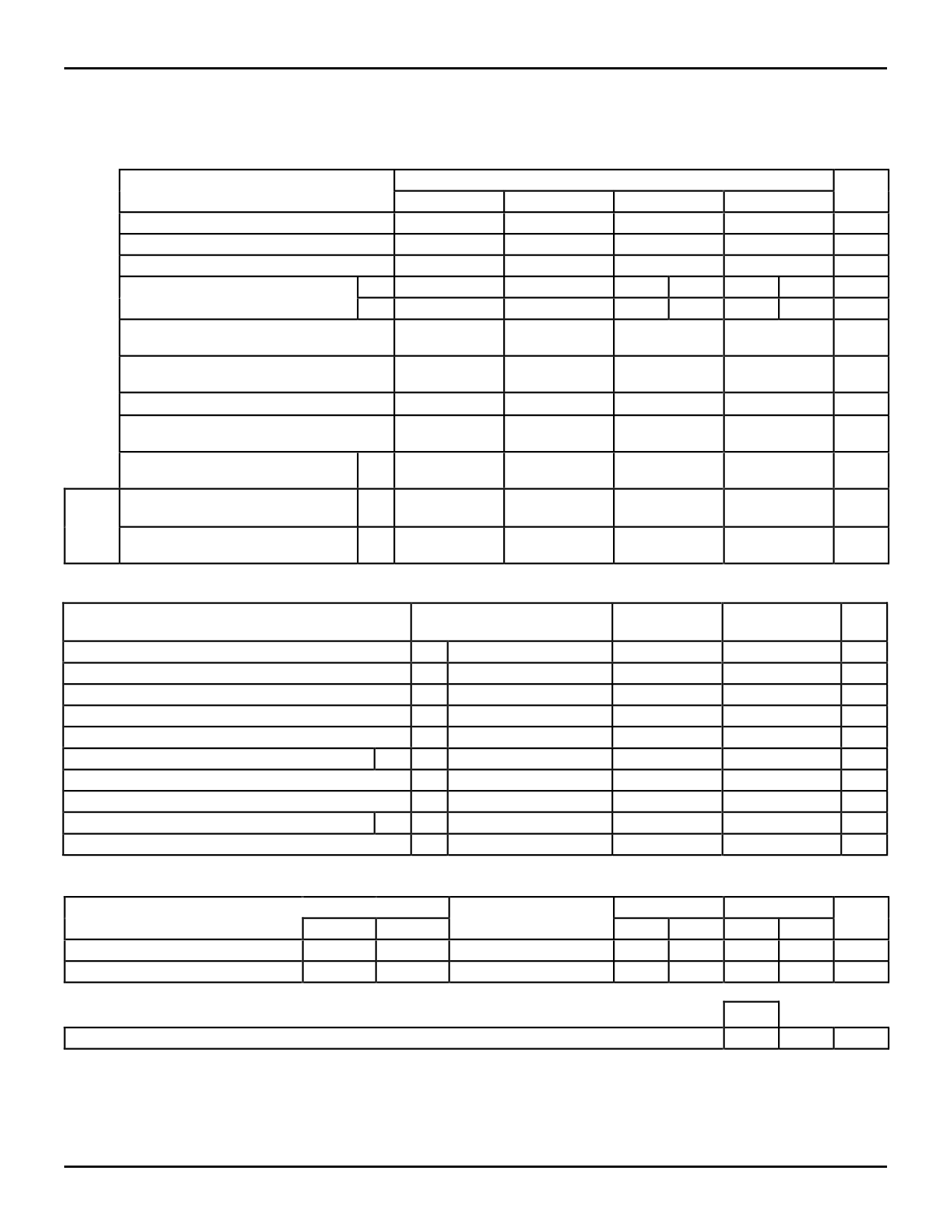
IDT49C460A AC ELECTRICAL CHARACTERISTICS
(Guaranteed Commercial Range Performance) Temperature range: 0°C to 70°C, VCC = 5.0V ± 5%
The inputs switch between 0V to 3V with signal measured at the 1.5V level.
PROPAGATION DELAYS(1)
From Input
DATA0–31 (3)
CB0–7 (CODE ID1,0 = 00, 11)
CB0–7 (CODE ID1,0 = 10)
LEOUT/GENERATE
CORRECT
Not Internal Control Mode
DIAG MODE
Not Internal Control Mode
CODE ID1,0
SC0–7
27
16
16
u
—
d
21
—
17
18
To Output
DATA0–31
ERROR
36(2)
30
34
19
20
—
12
d 25
—
u 25
23
—
26
20
26
21
MULT ERROR Unit
33
ns
23
ns
—
ns
d
25
ns
u
25
ns
—
ns
24
ns
26
ns
LEIN
27
38
30
From latched to Transparent
LEDIAG
u
15
29
19
From latched to Transparent
Internal LEDIAG
u
16
32
29
Control From latched to Transparent
Mode DATA0–31
u
16
32(2)
20
Via Diagnostic Latch
SET-UP AND HOLD TIMES RELATIVE TO LATCH ENABLES
33
ns
22
ns
24
ns
25
ns
2584 tbl 52
From Input
DATA0–31 (4)
CB0–7(4)
DATA0–31(4, 6)
CB0–7 (CODE ID 00, 11)(4, 6)
CB0–7 (CODE ID 10)(4, 6)
CORRECT(4, 6)
DIAG MODE(4, 6)
CODE ID1,0(4, 6)
LEIN(4, 6)
DATA0–31(4, 6)
To Input
(Latching Data)
d
d
d
d
d
ud
d
d
ud
LEIN
LEIN
LEOUT/GENERATE
LEOUT/GENERATE
LEOUT/GENERATE
LEOUT/GENERATE
LEOUT/GENERATE
LEOUT/GENERATE
LEOUT/GENERATE
LEDIAG
OUTPUT ENABLE/DISABLE TIMES(5)
Set-up Time
Min.
5
5
23
15
15
11
17
17
25
5
Hold Time
Min.
4
4
0
0
0
0
0
0
0
3
Unit
ns
ns
ns
ns
ns
ns
ns
ns
ns
ns
2584 tbl 53
From Input
OE Byte0–3
OESC
Enable
d
d
Disable
u
u
To Output
DATA0–31
SC0–7
Enable
Min. Max.
0
12
0
12
Disable
Min. Max.
0
14
0
14
Unit
ns
ns
2584 tbl 54
MINIMUM PULSE WIDTHS
ud LEIN, LEOUT/GENERATE, LEDIAG
(Positive–going pulse)
Min.
9
ns
NOTES:
2584 tbl 55
1. CI = 50pF.
2. These parameters are combinational propagation delay calculations, and are not tested in production.
3. Data In or Correct Data Out measurement requires timing as shown in the Switching Waveforms.
4. Set-up and Hold times relative to Latch Enables (Latching Data).
5. Output tests specified with CI = 5pF and measured to 0.5V change of output level. Testing is performed at CI = 50pF and correlated to CI = 5pF.
6. Not production tested, guaranteed by characterization.
11.6
25
Share Link: 