IDT6116LA55TD(2013) 데이터 시트보기 (PDF) - Integrated Device Technology
부품명
상세내역
제조사
IDT6116LA55TD Datasheet PDF : 11 Pages
| |||
IDT6116SA/LA
CMOS Static RAM 2K (16K x 8-Bit)
Military, Commercial, and Industrial Temperature Ranges
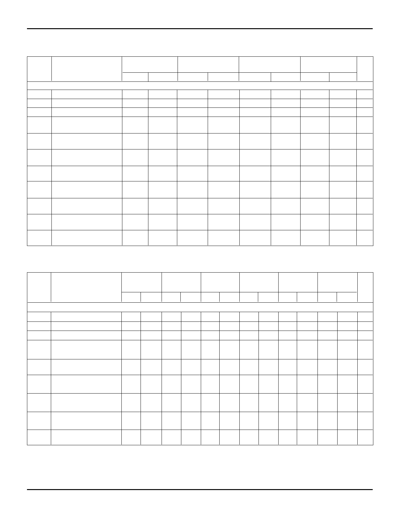
AC Electrical Characteristics (VCC = 5V ± 10%, All Temperature Ranges)
6116SA15(1)
6116SA20
6116LA20
6116SA25
6116LA25
6116SA35(2)
6116LA35(2)
Symbol
Parameter
Min. Max. Min. Max. Min. Max. Min. Max. Unit
Read Cycle
tRC
Read Cycle Time
tAA
Address Access Time
tACS
Chip Select Access Time
15
____
20
____
25
____
35
____
ns
____
15
____
19
____
25
____
35 ns
____
15
____
20
____
25
____
35 ns
tCLZ(3)
tOE
tOLZ(3)
Chip Select to Output in Low-Z
Output Enable to Output Valid
Output Enable to Output in Low-Z
5
____
5
____
5
____
5
____
ns
____
10
____
10
____
13
____
20 ns
0
____
0
____
5
____
5
____
ns
tCHZ(3)
Chip Deselect to Output in High-Z
____
10
____
11
____
12
____
15 ns
tOHZ(3)
tOH
Output Disable to Output in High-Z
Output Hold from Address Change
____
8
____
8
____
10
____
13 ns
5
____
5
____
5
____
5
____
ns
tPU(3)
Chip Select to Power Up Time
0
____
0
____
0
____
0
____
ns
tPD(3)
Chip Deselect to Power Down Time
____
15
____
20
____
25
____
35 ns
3089 tbl 12
AC Electrical Characteristics (VCC = 5V ± 10%, All Temperature Ranges) (continued)
6116SA45(2)
6116LA45(2)
6116SA55(2)
6116LA55(2)
6116SA70(2)
6116LA70(2)
6116SA90(2)
6116LA90(2)
6116SA120(2)
6116LA120(2)
6116SA150(2)
6116LA150(2)
Symbol
Parameter
Min. Max. Min. Max. Min. Max. Min. Max. Min. Max. Min. Max. Unit
Read Cycle
tRC
Read Cycle Time
45
____
55
____
70
____
90
____
120
____
150
____
ns
tAA
Address Access Time
____
45
____
55
____
70
____
90
____
120
____
150 ns
tACS
Chip Select Access Time
____
45
____
50
____
65
____
90
____
120
____
150 ns
tCLZ(3)
Chip Select to Output in Low-Z
5
____
5
____
5
____
5
____
5
____
5
____
ns
tOE
Output Enable to Output Valid
____
25
____
40
____
50
____
60
____
80
____
100 ns
tOLZ(3)
Output Enable to Output in Low-Z
5
____
5
____
5
____
5
____
5
____
5
____
ns
tCHZ(3)
Chip Deselect to Output in High-Z
____
20
____
30
____
35
____
40
____
40
____
40 ns
tOHZ(3)
Output Disable to Output in High-Z
____
15
____
30
____
35
____
40
____
40
____
40 ns
tOH
Output Hold from Address Change
5
____
5
____
5
____
5
____
5
____
5
____
ns
3089 tbl 13
NOTES:
1. 0°C to +70°C temperature range only.
2. –55°C to +125°C temperature range only.
3. This parameter guaranteed with the AC Load (Figure 2) by device characterization, but is not production tested.
6
Share Link: 